Architectures Numeriques Avancees VHDL - Semestre 7
Annee Universitaire : 2023-2024
Semestre : 7
Credits : 2.5 ECTS
Specialite : Conception Numerique et FPGA
PART A - Presentation Generale du Module
Vue d'ensemble
Ce cours enseigne la conception de systemes numeriques complexes avec le langage VHDL (VHSIC Hardware Description Language) et leur implementation sur FPGA. Il couvre la conception d'architectures numeriques avancees : unite arithmetique et logique (ALU), bancs de registres, memoires, et processeurs complets.
Objectifs pedagogiques :
- Maitriser le langage VHDL pour la description materielle
- Concevoir des circuits numeriques synthetisables
- Implementer des systemes sur FPGA (Xilinx)
- Simuler et verifier des designs avec testbenches
- Comprendre les machines a etats finis (FSM)
- Concevoir un processeur simple complet
Position dans le cursus
Ce module s'appuie sur :
- Fondements electronique numerique (S5) : portes logiques, bascules
- Logique sequentielle (S5) : machines a etats, compteurs
- Architecture Informatique materielle (S5) : structure processeur
Il prepare a :
- Systemes embarques : accelerateurs materiels
- Traitement du signal sur FPGA : implementation de filtres numeriques
- Conception ASIC : circuits integres specialises
- Systemes temps reel : logique cablee haute performance
PART B - Experience Personnelle et Contexte d'Apprentissage
Organisation et ressources
Le module etait organise en cours magistraux et bureau d'etudes pratique :
Cours magistraux (16h) :
- Syntaxe et structure VHDL
- Types de donnees et operateurs
- Logique combinatoire et sequentielle
- Machines a etats finis (FSM)
- Architectures de processeurs
Bureau d'etudes (20h) :
Projets de conception progressive avec Xilinx Vivado :
- Projet ALU : unite arithmetique et logique
- Projet registre : banc de registres
- Projet buffer : memoire tampon
- Projet memoire instruction : ROM pour code programme
- Projet memoire donnee : RAM pour donnees
- Projet processeur : integration complete
Devoirs maison :
- DM1 : ALU et testbench
- DM2 : Circuit numerique complexe
Outils utilises :
- Xilinx Vivado Design Suite (synthese, simulation, implementation)
- FPGA cible : probablement Artix-7 ou Zynq
- Testbenches VHDL pour simulation
- Waveform viewer (fichiers .wcfg)
Structure des projets
Chaque projet Vivado contenait :
- Sources : fichiers VHDL (sources_1/new/)
- Simulations : testbenches (sim_1/)
- Contraintes : fichiers .xdc pour mapping des pins (constrs_1/)
- Waveforms : fichiers .wcfg pour visualisation des signaux
- Synthese et implementation : runs/synth_1/, runs/impl_1/
Progression pedagogique :

Figure : Architecture d'un processeur simple en VHDL - ALU, registres et memoire
- Buffer : Circuit simple (FIFO ou registre a decalage)
- ALU : Operations arithmetiques et logiques
- Registre : Banc de registres avec lecture/ecriture
- Memoire instruction : ROM pour stocker le programme
- Memoire donnee : RAM pour stocker les donnees
- Processeur : Assemblage final (chemin de donnees + unite de controle)
Methode de travail
Phase 1 : Specification :
Definir l'interface (ports d'entree/sortie) et le comportement attendu du circuit.
Phase 2 : Code VHDL :
Ecrire le code dans Vivado, respecter les regles de synthetisabilite.
Phase 3 : Testbench :
Creer un testbench pour verifier fonctionnellement le circuit par simulation.
Phase 4 : Simulation :
Lancer la simulation comportementale, observer les chronogrammes (waveforms), corriger les erreurs.
Phase 5 : Synthese :
Verifier que le code se synthetise sans erreurs, analyser l'utilisation des ressources (LUT, FF, BRAM).
Phase 6 : Implementation (optionnel) :
Placer et router le design, verifier le timing, programmer le FPGA.
Difficultes rencontrees
Pensee parallele :
VHDL decrit du materiel ou tout s'execute en parallele, contrairement a la programmation sequentielle. Comprendre que les process s'executent simultanement demande un changement de paradigme.
Syntaxe stricte :
VHDL est verbeux et type fortement. Les erreurs de syntaxe ou de typage sont frequentes au debut.
Timing et synchronisation :
Gerer correctement les horloges, resets, et eviter les hazards (glitches) necessite de la rigueur.
Debugging :
Sans printf ni debogueur, le debugging se fait via les chronogrammes. Savoir quels signaux observer est crucial.
PART C - Aspects Techniques Detailles
1. Introduction au VHDL
VHDL = VHSIC Hardware Description Language
VHSIC = Very High Speed Integrated Circuit
Langage de description materielle :
- Decrit la structure et le comportement de circuits numeriques
- Utilise pour simulation et synthese (generation de circuits reels)
- Standard IEEE (IEEE 1076)
Difference programmation logicielle :
| Aspect | Logiciel | Materiel (VHDL) |
|---|---|---|
| Execution | Sequentielle | Parallele |
| Variables | Modifiees en sequence | Signaux qui evoluent dans le temps |
| Boucles | Iterations | Replication de materiel |
| Ressources | Abstraites (memoire virtuelle) | Physiques limitees (LUT, FF) |
2. Structure d'un fichier VHDL
Entity (entite) :
Decrit l'interface du composant (ports d'entree/sortie).
Exemple :
entity compteur is
  port (
    clk    : in  std_logic;
    reset  : in  std_logic;
    enable : in  std_logic;
    count  : out std_logic_vector(7 downto 0)
  );
end entity compteur;
Architecture :
Decrit le comportement ou la structure interne du composant.
Exemple :
architecture behavioral of compteur is
  signal count_internal : unsigned(7 downto 0);
begin
  process(clk, reset)
  begin
    if reset = '1' then
      count_internal <= (others => '0');
    elsif rising_edge(clk) then
      if enable = '1' then
        count_internal <= count_internal + 1;
      end if;
    end if;
  end process;

  count <= std_logic_vector(count_internal);
end architecture behavioral;
Types d'architectures :
| Type | Description | Usage |
|---|---|---|
| Behavioral | Description algorithmique du comportement | Haut niveau, synthese automatique |
| Dataflow | Affectations concurrentes, equations | Logique combinatoire |
| Structural | Instanciation de composants | Hierarchie, connexion de blocs |
3. Types de donnees VHDL
Types standards :
| Type | Description | Exemple |
|---|---|---|
| std_logic | Bit logique (9 valeurs) | '0', '1', 'Z', 'X', etc. |
| std_logic_vector | Vecteur de bits | "10110101" |
| integer | Entier | -2147483648 a 2147483647 |
| unsigned | Entier non signe | utilise pour calculs arithmetiques |
| signed | Entier signe | complement a 2 |
Valeurs std_logic :
- '0' : niveau bas
- '1' : niveau haut
- 'Z' : haute impedance (trois etats)
- 'X' : inconnu (non initialise)
- '-' : don't care (synthese)
Bibliotheques necessaires :
library IEEE;
use IEEE.STD_LOGIC_1164.ALL;      -- std_logic, std_logic_vector
use IEEE.NUMERIC_STD.ALL;         -- unsigned, signed, conversion
use IEEE.STD_LOGIC_UNSIGNED.ALL;  -- operations sur std_logic_vector (ancien)
4. Logique combinatoire
Affectation concurrente :
Les affectations en dehors des process s'executent en parallele.
Exemples :
-- Porte AND
y <= a and b;

-- Multiplexeur
y <= a when sel = '0' else b;

-- Multiplexeur 4 vers 1
with sel select
  y <= a when "00",
       b when "01",
       c when "10",
       d when others;
Process combinatoire :
Pour decrire de la logique combinatoire dans un process :
process(a, b, c)  -- Liste de sensibilite : tous les signaux lus
begin
  if a = '1' then
    y <= b;
  else
    y <= c;
  end if;
end process;
Attention : Si un signal lu n'est pas dans la liste de sensibilite, le process ne se met pas a jour - difference simulation/synthese.
5. Logique sequentielle
Bascule D (D Flip-Flop) :
Element de base de la logique sequentielle. Memorise une valeur sur un front d'horloge.
process(clk)
begin
  if rising_edge(clk) then  -- Front montant
    q <= d;
  end if;
end process;
Avec reset asynchrone :
process(clk, reset)
begin
  if reset = '1' then       -- Reset prioritaire
    q <= '0';
  elsif rising_edge(clk) then
    q <= d;
  end if;
end process;
Avec reset synchrone :
process(clk)
begin
  if rising_edge(clk) then
    if reset = '1' then
      q <= '0';
    else
      q <= d;
    end if;
  end if;
end process;
Regle d'or :
- Reset asynchrone : dans la sensibilite du process et teste en premier
- Reset synchrone : a l'interieur du test de rising_edge
6. Machines a etats finis (FSM)
Definition :
Une FSM (Finite State Machine) est un circuit sequentiel avec un nombre fini d'etats. Elle change d'etat selon les entrees et l'etat courant.
Types :
- Moore : sorties dependent seulement de l'etat
- Mealy : sorties dependent de l'etat et des entrees
Structure a 2 process :
Process 1 : Registre d'etat (sequentiel)
process(clk, reset)
begin
  if reset = '1' then
    etat_courant <= IDLE;
  elsif rising_edge(clk) then
    etat_courant <= etat_suivant;
  end if;
end process;
Process 2 : Logique de transition (combinatoire)
process(etat_courant, entree)
begin
  case etat_courant is
    when IDLE =>
      if entree = '1' then
        etat_suivant <= TRAITEMENT;
      else
        etat_suivant <= IDLE;
      end if;
      sortie <= '0';

    when TRAITEMENT =>
      if compteur_fini = '1' then
        etat_suivant <= FIN;
      else
        etat_suivant <= TRAITEMENT;
      end if;
      sortie <= '1';

    when FIN =>
      etat_suivant <= IDLE;
      sortie <= '0';

    when others =>
      etat_suivant <= IDLE;
      sortie <= '0';
  end case;
end process;
Declaration des etats :
type etat_type is (IDLE, TRAITEMENT, FIN);
signal etat_courant, etat_suivant : etat_type;
7. Unite Arithmetique et Logique (ALU)
Principe :
L'ALU effectue les operations arithmetiques (addition, soustraction) et logiques (AND, OR, XOR) d'un processeur.
Interface typique :
entity ALU is
  port (
    A      : in  std_logic_vector(31 downto 0);  -- Operande A
    B      : in  std_logic_vector(31 downto 0);  -- Operande B
    OP     : in  std_logic_vector(3 downto 0);   -- Code operation
    Result : out std_logic_vector(31 downto 0);  -- Resultat
    Zero   : out std_logic;                      -- Flag zero
    Carry  : out std_logic                       -- Flag retenue
  );
end entity ALU;
Operations courantes :
| Code OP | Operation | Description |
|---|---|---|
| 0000 | AND | ET logique bit a bit |
| 0001 | OR | OU logique bit a bit |
| 0010 | ADD | Addition |
| 0110 | SUB | Soustraction (A - B) |
| 0111 | SLT | Set if Less Than (A < B) |
| 1100 | NOR | NON-OU logique |
Implementation :
process(A, B, OP)
  variable temp : unsigned(32 downto 0);  -- 33 bits pour la retenue
begin
  case OP is
    when "0000" =>  -- AND
      Result <= A and B;
      Carry <= '0';

    when "0001" =>  -- OR
      Result <= A or B;
      Carry <= '0';

    when "0010" =>  -- ADD
      temp := ('0' & unsigned(A)) + ('0' & unsigned(B));
      Result <= std_logic_vector(temp(31 downto 0));
      Carry <= temp(32);

    when "0110" =>  -- SUB
      temp := ('0' & unsigned(A)) - ('0' & unsigned(B));
      Result <= std_logic_vector(temp(31 downto 0));
      Carry <= temp(32);

    when others =>
      Result <= (others => '0');
      Carry <= '0';
  end case;

  -- Flag Zero
  if Result = x"00000000" then
    Zero <= '1';
  else
    Zero <= '0';
  end if;
end process;
8. Banc de registres
Principe :
Ensemble de registres (16 ou 32 typiquement) pour stocker temporairement des donnees dans un processeur.
Interface :
entity RegisterFile is
  port (
    clk       : in  std_logic;
    reset     : in  std_logic;
    -- Lecture
    ReadAddr1 : in  std_logic_vector(4 downto 0);   -- Adresse registre 1
    ReadAddr2 : in  std_logic_vector(4 downto 0);   -- Adresse registre 2
    ReadData1 : out std_logic_vector(31 downto 0);  -- Donnee registre 1
    ReadData2 : out std_logic_vector(31 downto 0);  -- Donnee registre 2
    -- Ecriture
    WriteEn   : in  std_logic;                      -- Autorisation ecriture
    WriteAddr : in  std_logic_vector(4 downto 0);   -- Adresse ecriture
    WriteData : in  std_logic_vector(31 downto 0)   -- Donnee a ecrire
  );
end entity RegisterFile;
Implementation :
architecture behavioral of RegisterFile is
  type reg_array is array (0 to 31) of std_logic_vector(31 downto 0);
  signal registers : reg_array;
begin
  -- Ecriture synchrone
  process(clk, reset)
  begin
    if reset = '1' then
      registers <= (others => (others => '0'));
    elsif rising_edge(clk) then
      if WriteEn = '1' and WriteAddr /= "00000" then  -- R0 toujours a 0
        registers(to_integer(unsigned(WriteAddr))) <= WriteData;
      end if;
    end if;
  end process;

  -- Lecture asynchrone
  ReadData1 <= registers(to_integer(unsigned(ReadAddr1)));
  ReadData2 <= registers(to_integer(unsigned(ReadAddr2)));
end architecture behavioral;
Particularite :
Le registre R0 est souvent cable a zero (convention MIPS/RISC-V).
9. Memoires
ROM (Read-Only Memory) :
Utilisee pour stocker le programme (instructions).
architecture behavioral of ROM is
  type rom_array is array (0 to 255) of std_logic_vector(31 downto 0);
  constant rom_data : rom_array := (
    x"00000000",  -- NOP
    x"20010005",  -- ADDI R1, R0, 5
    x"20020003",  -- ADDI R2, R0, 3
    x"00221820",  -- ADD R3, R1, R2
    -- ... autres instructions
    others => x"00000000"
  );
begin
  process(clk)
  begin
    if rising_edge(clk) then
      data_out <= rom_data(to_integer(unsigned(address)));
    end if;
  end process;
end architecture behavioral;
RAM (Random Access Memory) :
Utilisee pour stocker les donnees.
architecture behavioral of RAM is
  type ram_array is array (0 to 1023) of std_logic_vector(31 downto 0);
  signal ram_data : ram_array := (others => (others => '0'));
begin
  process(clk)
  begin
    if rising_edge(clk) then
      if write_enable = '1' then
        ram_data(to_integer(unsigned(address))) <= data_in;
      end if;
      data_out <= ram_data(to_integer(unsigned(address)));
    end if;
  end process;
end architecture behavioral;
Utilisation des BRAM (Block RAM) sur FPGA :
Les FPGA possedent des blocs memoire dedies (BRAM). Vivado infere automatiquement des BRAM si le code suit certains modeles (comme ci-dessus).
10. Processeur simple
Architecture :
Un processeur minimal contient :
- Chemin de donnees (Datapath) : ALU, registres, memoires, multiplexeurs
- Unite de controle : FSM qui genere les signaux de controle
Cycle d'execution :
- Fetch : Lire l'instruction en memoire (PC → Mem_Instr → IR)
- Decode : Decoder l'instruction (champs opcode, registres, immediat)
- Execute : Executer l'operation (ALU)
- Memory : Acces memoire donnees si necessaire (LOAD/STORE)
- Write Back : Ecrire le resultat dans le registre destination
Signaux de controle :
L'unite de controle genere des signaux pour piloter le datapath :
- RegWrite : autoriser ecriture dans le banc de registres
- ALUOp : selection operation ALU
- MemRead, MemWrite : lecture/ecriture memoire donnees
- MemToReg : selection source donnee a ecrire dans registre
- Branch : autoriser branchement conditionnel
Exemple simplifie :
Type d'instruction R (registre-registre) :
- Opcode determine que c'est une instruction R
- Lire deux registres sources (rs, rt)
- ALU effectue l'operation (funct determine laquelle)
- Ecrire le resultat dans registre destination (rd)
11. Testbench et simulation
Testbench :
Fichier VHDL sans ports (entity vide) qui instancie le circuit a tester (UUT - Unit Under Test) et genere des stimuli.
Structure :
entity testbench is
  -- Pas de ports
end entity testbench;

architecture test of testbench is
  -- Declaration des signaux de test
  signal clk : std_logic := '0';
  signal reset : std_logic := '1';
  signal input : std_logic_vector(7 downto 0);
  signal output : std_logic_vector(7 downto 0);

  constant CLK_PERIOD : time := 10 ns;
begin
  -- Instanciation du composant a tester
  UUT: entity work.mon_circuit
    port map (
      clk => clk,
      reset => reset,
      input => input,
      output => output
    );

  -- Generation de l'horloge
  clk_process: process
  begin
    clk <= '0';
    wait for CLK_PERIOD/2;
    clk <= '1';
    wait for CLK_PERIOD/2;
  end process;

  -- Generation des stimuli
  stim_process: process
  begin
    reset <= '1';
    input <= x"00";
    wait for 50 ns;

    reset <= '0';
    wait for 10 ns;

    input <= x"12";
    wait for 20 ns;

    input <= x"34";
    wait for 20 ns;

    wait;  -- Arret de la simulation
  end process;
end architecture test;
Verifications :
Utiliser des assertions pour verifier automatiquement :
assert (output = x"46") report "Erreur : resultat incorrect" severity error;Waveform (chronogramme) :
Fichiers .wcfg dans Vivado permettent de configurer quels signaux afficher et comment. Essentiels pour le debugging visuel.
12. Synthese et implementation sur FPGA
Etapes :
1. Synthese (Synthesis) :
- Conversion du code VHDL en netlist (portes logiques)
- Optimisation logique
- Verification que le code est synthetisable
2. Implementation :
- Placement : affecter les ressources logiques aux elements du FPGA (LUT, FF)
- Routage : connecter les elements via les interconnexions
- Verification timing : s'assurer que les contraintes temporelles sont respectees
3. Generation du bitstream :
- Fichier .bit a programmer dans le FPGA
Ressources FPGA :
| Ressource | Description |
|---|---|
| LUT (Look-Up Table) | Implemente logique combinatoire (fonction quelconque de N entrees) |
| FF (Flip-Flop) | Bascule D pour logique sequentielle |
| BRAM (Block RAM) | Blocs memoire dedies (18 Kb ou 36 Kb) |
| DSP | Blocs multiplicateurs/accumulateurs materiels |
| IO | Broches d'entree/sortie configurables |
Contraintes :
Fichier .xdc (Xilinx Design Constraints) :
- Affectation des pins physiques
- Definition des horloges (periode, frequence)
- Contraintes de timing
Exemple :
# Horloge 100 MHz
create_clock -period 10.000 -name clk [get_ports clk]

# Pins
set_property PACKAGE_PIN W5 [get_ports clk]
set_property IOSTANDARD LVCMOS33 [get_ports clk]

set_property PACKAGE_PIN U16 [get_ports led[0]]
set_property IOSTANDARD LVCMOS33 [get_ports led[0]]
PART D - Analyse Reflexive et Perspectives
Competences acquises
Conception materielle :
Maitrise du VHDL pour decrire des circuits numeriques synthetisables. Capacite a penser en termes de parallelisme materiel plutot que sequence logicielle.
Architecture de processeur :
Comprehension profonde du fonctionnement interne d'un processeur : ALU, registres, memoires, unite de controle, chemin de donnees.
Outils professionnels :
Utilisation de Xilinx Vivado, outil standard de l'industrie pour FPGA. Simulation, synthese, implementation, analyse de timing.
Points cles a retenir
1. VHDL = description materielle, pas programmation :
Le code VHDL decrit du materiel qui existe physiquement. Tout s'execute en parallele. Changement de paradigme fondamental.
2. Synthetisabilite :
Tout le code VHDL ne peut pas etre synthetise en materiel. Eviter wait for (sauf dans testbenches), boucles infinies, division par variables, etc.
3. Horloge et synchronisme :
Les circuits synchrones (cadences par horloge) sont plus robustes et previsibles. Toujours utiliser rising_edge(clk) pour detecter les fronts.
4. Testbench = essentiel :
La simulation avec testbench permet de valider le fonctionnement avant synthese. Debug beaucoup plus facile qu'apres implementation.
5. Ressources limitees :
Les FPGA ont un nombre fini de LUT, FF, BRAM. Importance de l'optimisation et du partage de ressources.
Applications pratiques
Traitement du signal :
Implementation de filtres numeriques haute performance (FIR, IIR), FFT, traitement d'image temps reel.
Accelerateurs materiels :
Acceleration de calculs intensifs (cryptographie, compression, IA) en dechargeant le processeur.
Systemes embarques critiques :
Aeronautique, automobile, spatial necessitent des circuits deterministes et fiables (logique cablee sur FPGA ou ASIC).
Prototypage ASIC :
Les FPGA servent a valider des designs avant fabrication d'ASIC (cout eleve, non modifiable).
Retour d'experience
Courbe d'apprentissage :
VHDL est plus difficile que la programmation classique au debut. Necessite de comprendre le materiel sous-jacent.
Projets progressifs :
La progression Buffer → ALU → Registres → Memoires → Processeur est pedagogiquement excellente. Chaque etape ajoute de la complexite.
Vivado puissant mais complexe :
L'outil est complet mais l'interface peut etre intimidante. Temps de synthese/implementation parfois long.
Debugging visuel :
Les waveforms (chronogrammes) sont indispensables. Savoir identifier les signaux critiques a observer facilite grandement le debugging.
Limites et ouvertures
Limites du module :
- Pas d'implementation physique sur carte FPGA (simulation seulement)
- Processeur tres simplifie (pas de pipeline, cache, etc.)
- Aspects timing et optimisation peu approfondis
Ouvertures vers :
- Processeurs avances : pipeline, prediction de branchement, cache
- Systemes sur puce (SoC) : processeur + peripheriques integres
- High-Level Synthesis (HLS) : generer VHDL depuis C/C++
- Verification formelle : assertions, model checking
- ASIC design : conception de circuits integres application specifique
Evolution technologique
Tendances actuelles :
HLS (High-Level Synthesis) :
Outils comme Vivado HLS ou Vitis HLS permettent d'ecrire en C/C++ et generent automatiquement du VHDL/Verilog. Accelere le developpement.
FPGA + IA :
Les FPGA modernes (Versal, Zynq UltraScale+) integrent des accelerateurs IA (DPU). Utilises pour inference de reseaux de neurones temps reel.
FPGA adaptatives (Versal) :
Architecture hybride : FPGA + CPU + DSP + IA. Reconfiguration dynamique.
Cloud FPGA :
AWS, Azure, Alibaba proposent des instances avec FPGA pour acceleration dans le cloud.
Conseils pour reussir
1. Penser materiel :
Visualiser mentalement les portes, bascules, multiplexeurs generes par votre code VHDL.
2. Simuler tot et souvent :
Ne pas attendre d'avoir ecrit tout le code. Tester chaque module independamment.
3. Bien commenter :
VHDL est verbeux. Des commentaires clairs aident a relire le code plus tard.
4. Respecter les conventions :
Noms de signaux explicites (clk, reset, enable), indentation coherente.
5. Utiliser les types appropries :
unsigned/signed pour arithmetique, std_logic_vector pour bus de donnees generiques.
Conclusion
Ce module fournit une excellente introduction a la conception numerique avec VHDL et FPGA. La realisation d'un processeur complet, meme simple, permet de comprendre en profondeur l'architecture des ordinateurs.
Competences transferables :
- Pensee parallele et conception materielle
- Rigueur dans la specification et la verification
- Maitrise d'outils professionnels (Vivado)
- Comprehension de l'architecture des processeurs
Pertinence professionnelle :
Les FPGA sont utilises dans de nombreux domaines (telecommunications, defense, medical, automobile, finance). La demande en ingenieurs FPGA reste forte.
Message principal :
VHDL et les FPGA offrent un controle total sur le materiel, permettant des performances et une efficacite energetique inatteignables avec du logiciel seul. La maitrise de ces outils ouvre des opportunites dans les systemes haute performance.
Recommandations :
- Pratiquer sur des cartes FPGA reelles (Basys, Arty, DE10-Nano)
- Explorer des projets plus complexes (controleurs, interfaces, DSP)
- Apprendre Verilog en complement (langage concurrent)
- Se former au HLS pour accelerer le developpement
- Etudier l'architecture de processeurs reels (RISC-V open-source)
Liens avec les autres cours :
- Architecture Informatique materielle - S5 : structure processeur
- Fondements electronique numerique - S5 : portes logiques
- Embedded IA for IoT - S9 : acceleration materielle
Illustrations du Projet BE Pipeline
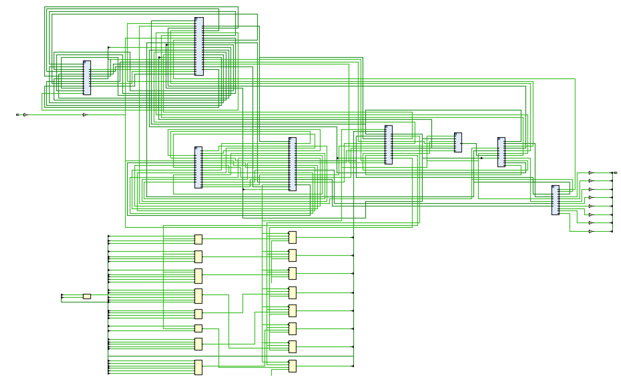
Figure : Chemin de donnees (Datapath) du processeur pipeline
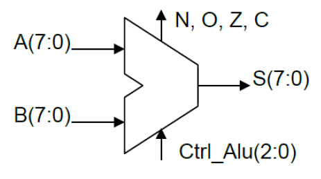
Figure : Schema de l'Unite Arithmetique et Logique (ALU)
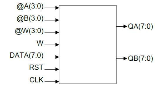
Figure : Banc de registres (Register Bench)
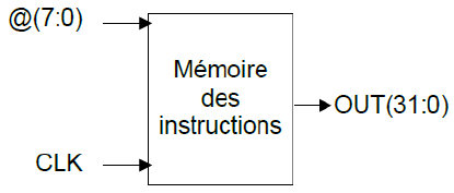
Figure : Memoire d'instructions (Instruction Memory)
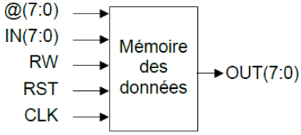
Figure : Memoire de donnees (Data Memory)
Figure : Gestion des aleas (hazards) dans le pipeline
Rapports et Projets
Rapport de Projet VHDLVHDL Project Report
Rapport du bureau d'etudes : conception d'un processeur pipeline en VHDL, incluant ALU, banc de registres, memoires et gestion des aleas.Design study report: pipeline processor design in VHDL, including ALU, register file, memories and hazard management.
Documents de CoursCourse Documents
Cours VHDL CompletComplete VHDL Course
Cours complet de VHDL : syntaxe, processus, machines a etats, simulation et synthese pour FPGA.Complete VHDL course: syntax, processes, state machines, simulation and synthesis for FPGA.
Projet Processeur RISCRISC Processor Project
Sujet du projet BE : conception d'un microprocesseur RISC en VHDL avec ALU, banc de registres et memoire.Design study project brief: RISC microprocessor design in VHDL with ALU, register file and memory.
Cours suivi en 2023-2024 a l'INSA Toulouse, Departement Genie Electrique et Informatique.
Advanced Digital Architectures VHDL - Semester 7
Academic Year: 2023-2024
Semester: 7
Credits: 2.5 ECTS
Specialization: Digital Design and FPGA
PART A - General Module Presentation
Overview
This course teaches the design of complex digital systems using the VHDL language (VHSIC Hardware Description Language) and their implementation on FPGA. It covers the design of advanced digital architectures: arithmetic and logic unit (ALU), register files, memories, and complete processors.
Learning objectives:
- Master the VHDL language for hardware description
- Design synthesizable digital circuits
- Implement systems on FPGA (Xilinx)
- Simulate and verify designs with testbenches
- Understand finite state machines (FSM)
- Design a complete simple processor
Position in the curriculum
This module builds upon:
- Digital Electronics Fundamentals (S5): logic gates, flip-flops
- Sequential Logic (S5): state machines, counters
- Hardware Computer Architecture (S5): processor structure
It prepares for:
- Embedded systems: hardware accelerators
- Signal processing on FPGA: digital filter implementation
- ASIC design: specialized integrated circuits
- Real-time systems: high-performance hardwired logic
PART B - Personal Experience and Learning Context
Organization and resources
The module was organized into lectures and practical design studies:
Lectures (16h):
- VHDL syntax and structure
- Data types and operators
- Combinational and sequential logic
- Finite state machines (FSM)
- Processor architectures
Design studies (20h):
Progressive design projects with Xilinx Vivado:
- ALU project: arithmetic and logic unit
- Register project: register file
- Buffer project: buffer memory
- Instruction memory project: ROM for program code
- Data memory project: RAM for data
- Processor project: complete integration
Homework assignments:
- HW1: ALU and testbench
- HW2: Complex digital circuit
Tools used:
- Xilinx Vivado Design Suite (synthesis, simulation, implementation)
- Target FPGA: likely Artix-7 or Zynq
- VHDL testbenches for simulation
- Waveform viewer (.wcfg files)
Project structure
Each Vivado project contained:
- Sources: VHDL files (sources_1/new/)
- Simulations: testbenches (sim_1/)
- Constraints: .xdc files for pin mapping (constrs_1/)
- Waveforms: .wcfg files for signal visualization
- Synthesis and implementation: runs/synth_1/, runs/impl_1/
Pedagogical progression:
Figure: Architecture of a simple VHDL processor - ALU, registers and memory
- Buffer: Simple circuit (FIFO or shift register)
- ALU: Arithmetic and logic operations
- Register: Register file with read/write
- Instruction memory: ROM for storing the program
- Data memory: RAM for storing data
- Processor: Final assembly (datapath + control unit)
Working method
Phase 1: Specification:
Define the interface (input/output ports) and the expected behavior of the circuit.
Phase 2: VHDL Code:
Write the code in Vivado, comply with synthesizability rules.
Phase 3: Testbench:
Create a testbench to functionally verify the circuit through simulation.
Phase 4: Simulation:
Run behavioral simulation, observe waveforms, correct errors.
Phase 5: Synthesis:
Verify that the code synthesizes without errors, analyze resource utilization (LUT, FF, BRAM).
Phase 6: Implementation (optional):
Place and route the design, verify timing, program the FPGA.
Challenges encountered
Parallel thinking:
VHDL describes hardware where everything executes in parallel, unlike sequential programming. Understanding that processes execute simultaneously requires a paradigm shift.
Strict syntax:
VHDL is verbose and strongly typed. Syntax and type errors are frequent at first.
Timing and synchronization:
Correctly managing clocks, resets, and avoiding hazards (glitches) requires rigor.
Debugging:
Without printf or debugger, debugging is done through waveforms. Knowing which signals to observe is crucial.
PART C - Detailed Technical Aspects
1. Introduction to VHDL
VHDL = VHSIC Hardware Description Language
VHSIC = Very High Speed Integrated Circuit
Hardware description language:
- Describes the structure and behavior of digital circuits
- Used for simulation and synthesis (real circuit generation)
- IEEE Standard (IEEE 1076)
Difference from software programming:
| Aspect | Software | Hardware (VHDL) |
|---|---|---|
| Execution | Sequential | Parallel |
| Variables | Modified sequentially | Signals that evolve over time |
| Loops | Iterations | Hardware replication |
| Resources | Abstract (virtual memory) | Limited physical (LUT, FF) |
2. Structure of a VHDL file
Entity:
Describes the component interface (input/output ports).
Example:
entity compteur is
  port (
    clk    : in  std_logic;
    reset  : in  std_logic;
    enable : in  std_logic;
    count  : out std_logic_vector(7 downto 0)
  );
end entity compteur;Architecture:
Describes the behavior or internal structure of the component.
Example:
architecture behavioral of compteur is
  signal count_internal : unsigned(7 downto 0);
begin
  process(clk, reset)
  begin
    if reset = '1' then
      count_internal <= (others => '0');
    elsif rising_edge(clk) then
      if enable = '1' then
        count_internal <= count_internal + 1;
      end if;
    end if;
  end process;

  count <= std_logic_vector(count_internal);
end architecture behavioral;
Architecture types:
| Type | Description | Usage |
|---|---|---|
| Behavioral | Algorithmic description of behavior | High level, automatic synthesis |
| Dataflow | Concurrent assignments, equations | Combinational logic |
| Structural | Component instantiation | Hierarchy, block connection |
3. VHDL data types
Standard types:
| Type | Description | Example |
|---|---|---|
| std_logic | Logic bit (9 values) | '0', '1', 'Z', 'X', etc. |
| std_logic_vector | Bit vector | "10110101" |
| integer | Integer | -2147483648 to 2147483647 |
| unsigned | Unsigned integer | used for arithmetic calculations |
| signed | Signed integer | two's complement |
std_logic values:
- '0': low level
- '1': high level
- 'Z': high impedance (tri-state)
- 'X': unknown (uninitialized)
- '-': don't care (synthesis)
Required libraries:
library IEEE;
use IEEE.STD_LOGIC_1164.ALL;      -- std_logic, std_logic_vector
use IEEE.NUMERIC_STD.ALL;         -- unsigned, signed, conversion
use IEEE.STD_LOGIC_UNSIGNED.ALL;  -- operations on std_logic_vector (legacy)
4. Combinational logic
Concurrent assignment:
Assignments outside processes execute in parallel.
Examples:
-- AND gate
y <= a and b;

-- Multiplexer
y <= a when sel = '0' else b;

-- 4-to-1 multiplexer
with sel select
  y <= a when "00",
       b when "01",
       c when "10",
       d when others;
Combinational process:
To describe combinational logic within a process:
process(a, b, c)  -- Sensitivity list: all signals read
begin
  if a = '1' then
    y <= b;
  else
    y <= c;
  end if;
end process;Warning: If a read signal is not in the sensitivity list, the process does not update - simulation/synthesis mismatch.
5. Sequential logic
D Flip-Flop:
Basic element of sequential logic. Stores a value on a clock edge.
process(clk)
begin
  if rising_edge(clk) then  -- Rising edge
    q <= d;
  end if;
end process;
With asynchronous reset:
process(clk, reset)
begin
  if reset = '1' then       -- Reset has priority
    q <= '0';
  elsif rising_edge(clk) then
    q <= d;
  end if;
end process;
With synchronous reset:
process(clk)
begin
  if rising_edge(clk) then
    if reset = '1' then
      q <= '0';
    else
      q <= d;
    end if;
  end if;
end process;
Golden rule:
- Asynchronous reset: in the process sensitivity list and tested first
- Synchronous reset: inside the rising_edge test
6. Finite State Machines (FSM)
Definition:
An FSM (Finite State Machine) is a sequential circuit with a finite number of states. It changes state based on inputs and the current state.
Types:
- Moore: outputs depend only on the state
- Mealy: outputs depend on the state and the inputs
2-process structure:
Process 1: State register (sequential)
process(clk, reset)
begin
  if reset = '1' then
    etat_courant <= IDLE;
  elsif rising_edge(clk) then
    etat_courant <= etat_suivant;
  end if;
end process;
Process 2: Transition logic (combinational)
process(etat_courant, entree)
begin
  case etat_courant is
    when IDLE =>
      if entree = '1' then
        etat_suivant <= TRAITEMENT;
      else
        etat_suivant <= IDLE;
      end if;
      sortie <= '0';

    when TRAITEMENT =>
      if compteur_fini = '1' then
        etat_suivant <= FIN;
      else
        etat_suivant <= TRAITEMENT;
      end if;
      sortie <= '1';

    when FIN =>
      etat_suivant <= IDLE;
      sortie <= '0';

    when others =>
      etat_suivant <= IDLE;
      sortie <= '0';
  end case;
end process;
State declaration:
type etat_type is (IDLE, TRAITEMENT, FIN);
signal etat_courant, etat_suivant : etat_type;
7. Arithmetic and Logic Unit (ALU)
Principle:
The ALU performs the arithmetic operations (addition, subtraction) and logic operations (AND, OR, XOR) of a processor.
Typical interface:
entity ALU is
  port (
    A      : in  std_logic_vector(31 downto 0);  -- Operand A
    B      : in  std_logic_vector(31 downto 0);  -- Operand B
    OP     : in  std_logic_vector(3 downto 0);   -- Operation code
    Result : out std_logic_vector(31 downto 0);  -- Result
    Zero   : out std_logic;                      -- Zero flag
    Carry  : out std_logic                       -- Carry flag
  );
end entity ALU;
Common operations:
| OP Code | Operation | Description |
|---|---|---|
| 0000 | AND | Bitwise logical AND |
| 0001 | OR | Bitwise logical OR |
| 0010 | ADD | Addition |
| 0110 | SUB | Subtraction (A - B) |
| 0111 | SLT | Set if Less Than (A < B) |
| 1100 | NOR | Logical NOR |
Implementation:
process(A, B, OP)
  variable temp : unsigned(32 downto 0);  -- 33 bits for carry
begin
  case OP is
    when "0000" =>  -- AND
      Result <= A and B;
      Carry <= '0';

    when "0001" =>  -- OR
      Result <= A or B;
      Carry <= '0';

    when "0010" =>  -- ADD
      temp := ('0' & unsigned(A)) + ('0' & unsigned(B));
      Result <= std_logic_vector(temp(31 downto 0));
      Carry <= temp(32);

    when "0110" =>  -- SUB
      temp := ('0' & unsigned(A)) - ('0' & unsigned(B));
      Result <= std_logic_vector(temp(31 downto 0));
      Carry <= temp(32);

    when others =>
      Result <= (others => '0');
      Carry <= '0';
  end case;

  -- Zero Flag
  if Result = x"00000000" then
    Zero <= '1';
  else
    Zero <= '0';
  end if;
end process;
8. Register file
Principle:
A set of registers (typically 16 or 32) for temporarily storing data in a processor.
Interface:
entity RegisterFile is
  port (
    clk       : in  std_logic;
    reset     : in  std_logic;
    -- Read
    ReadAddr1 : in  std_logic_vector(4 downto 0);   -- Register 1 address
    ReadAddr2 : in  std_logic_vector(4 downto 0);   -- Register 2 address
    ReadData1 : out std_logic_vector(31 downto 0);  -- Register 1 data
    ReadData2 : out std_logic_vector(31 downto 0);  -- Register 2 data
    -- Write
    WriteEn   : in  std_logic;                      -- Write enable
    WriteAddr : in  std_logic_vector(4 downto 0);   -- Write address
    WriteData : in  std_logic_vector(31 downto 0)   -- Data to write
  );
end entity RegisterFile;Implementation:
architecture behavioral of RegisterFile is
  type reg_array is array (0 to 31) of std_logic_vector(31 downto 0);
  signal registers : reg_array;
begin
  -- Synchronous write
  process(clk, reset)
  begin
    if reset = '1' then
      registers <= (others => (others => '0'));
    elsif rising_edge(clk) then
      if WriteEn = '1' and WriteAddr /= "00000" then  -- R0 always 0
        registers(to_integer(unsigned(WriteAddr))) <= WriteData;
      end if;
    end if;
  end process;

  -- Asynchronous read
  ReadData1 <= registers(to_integer(unsigned(ReadAddr1)));
  ReadData2 <= registers(to_integer(unsigned(ReadAddr2)));
end architecture behavioral;
Special note:
Register R0 is often hardwired to zero (MIPS/RISC-V convention).
9. Memories
ROM (Read-Only Memory):
Used for storing the program (instructions).
architecture behavioral of ROM is
  type rom_array is array (0 to 255) of std_logic_vector(31 downto 0);
  constant rom_data : rom_array := (
    x"00000000",  -- NOP
    x"20010005",  -- ADDI R1, R0, 5
    x"20020003",  -- ADDI R2, R0, 3
    x"00221820",  -- ADD R3, R1, R2
    -- ... other instructions
    others => x"00000000"
  );
begin
  process(clk)
  begin
    if rising_edge(clk) then
      data_out <= rom_data(to_integer(unsigned(address)));
    end if;
  end process;
end architecture behavioral;
RAM (Random Access Memory):
Used for storing data.
architecture behavioral of RAM is
  type ram_array is array (0 to 1023) of std_logic_vector(31 downto 0);
  signal ram_data : ram_array := (others => (others => '0'));
begin
  process(clk)
  begin
    if rising_edge(clk) then
      if write_enable = '1' then
        ram_data(to_integer(unsigned(address))) <= data_in;
      end if;
      data_out <= ram_data(to_integer(unsigned(address)));
    end if;
  end process;
end architecture behavioral;
Using BRAM (Block RAM) on FPGA:
FPGAs have dedicated memory blocks (BRAM). Vivado automatically infers BRAM if the code follows certain patterns (as shown above).
10. Simple processor
Architecture:
A minimal processor contains:
- Datapath: ALU, registers, memories, multiplexers
- Control unit: FSM that generates control signals
Execution cycle:
- Fetch: Read the instruction from memory (PC → Instr_Mem → IR)
- Decode: Decode the instruction (opcode, register, immediate fields)
- Execute: Execute the operation (ALU)
- Memory: Data memory access if needed (LOAD/STORE)
- Write Back: Write the result to the destination register
Control signals:
The control unit generates signals to drive the datapath:
- RegWrite: enable writing to the register file
- ALUOp: ALU operation selection
- MemRead, MemWrite: data memory read/write
- MemToReg: data source selection for register write
- Branch: enable conditional branching
Simplified example:
R-type instruction (register-register):
- Opcode determines it is an R-type instruction
- Read two source registers (rs, rt)
- ALU performs the operation (funct determines which one)
- Write the result to the destination register (rd)
11. Testbench and simulation
Testbench:
A VHDL file with no ports (empty entity) that instantiates the circuit under test (UUT - Unit Under Test) and generates stimuli.
Structure:
entity testbench is
  -- No ports
end entity testbench;

architecture test of testbench is
  -- Test signal declarations
  signal clk : std_logic := '0';
  signal reset : std_logic := '1';
  signal input : std_logic_vector(7 downto 0);
  signal output : std_logic_vector(7 downto 0);

  constant CLK_PERIOD : time := 10 ns;
begin
  -- Instantiation of the component under test
  UUT: entity work.mon_circuit
    port map (
      clk => clk,
      reset => reset,
      input => input,
      output => output
    );

  -- Clock generation
  clk_process: process
  begin
    clk <= '0';
    wait for CLK_PERIOD/2;
    clk <= '1';
    wait for CLK_PERIOD/2;
  end process;

  -- Stimulus generation
  stim_process: process
  begin
    reset <= '1';
    input <= x"00";
    wait for 50 ns;

    reset <= '0';
    wait for 10 ns;

    input <= x"12";
    wait for 20 ns;

    input <= x"34";
    wait for 20 ns;

    wait;  -- Stop simulation
  end process;
end architecture test;Verification:
Use assertions for automatic checking:
assert (output = x"46") report "Error: incorrect result" severity error;Waveform:
.wcfg files in Vivado allow configuring which signals to display and how. Essential for visual debugging.
12. Synthesis and implementation on FPGA
Steps:
1. Synthesis:
- Conversion of VHDL code into a netlist (logic gates)
- Logic optimization
- Verification that the code is synthesizable
2. Implementation:
- Placement: assign logic resources to FPGA elements (LUT, FF)
- Routing: connect elements through interconnections
- Timing verification: ensure timing constraints are met
3. Bitstream generation:
- .bit file to be programmed into the FPGA
FPGA resources:
| Resource | Description |
|---|---|
| LUT (Look-Up Table) | Implements combinational logic (arbitrary function of N inputs) |
| FF (Flip-Flop) | D flip-flop for sequential logic |
| BRAM (Block RAM) | Dedicated memory blocks (18 Kb or 36 Kb) |
| DSP | Hardware multiplier/accumulator blocks |
| IO | Configurable input/output pins |
Constraints:
.xdc file (Xilinx Design Constraints):
- Physical pin assignment
- Clock definition (period, frequency)
- Timing constraints
Example:
# 100 MHz clock
create_clock -period 10.000 -name clk [get_ports clk]

# Pins
set_property PACKAGE_PIN W5 [get_ports clk]
set_property IOSTANDARD LVCMOS33 [get_ports clk]

set_property PACKAGE_PIN U16 [get_ports led[0]]
set_property IOSTANDARD LVCMOS33 [get_ports led[0]]
PART D - Reflective Analysis and Perspectives
Skills acquired
Hardware design:
Mastery of VHDL for describing synthesizable digital circuits. Ability to think in terms of hardware parallelism rather than software sequences.
Processor architecture:
Deep understanding of a processor's internal workings: ALU, registers, memories, control unit, datapath.
Professional tools:
Use of Xilinx Vivado, industry-standard tool for FPGA. Simulation, synthesis, implementation, timing analysis.
Key takeaways
1. VHDL = hardware description, not programming:
VHDL code describes hardware that physically exists. Everything executes in parallel. A fundamental paradigm shift.
2. Synthesizability:
Not all VHDL code can be synthesized into hardware. Avoid wait for (except in testbenches), infinite loops, division by variables, etc.
3. Clock and synchronism:
Synchronous circuits (clocked) are more robust and predictable. Always use rising_edge(clk) to detect edges.
4. Testbench = essential:
Simulation with testbench allows validating functionality before synthesis. Debugging is much easier than after implementation.
5. Limited resources:
FPGAs have a finite number of LUTs, FFs, BRAMs. Optimization and resource sharing are important.
Practical applications
Signal processing:
Implementation of high-performance digital filters (FIR, IIR), FFT, real-time image processing.
Hardware accelerators:
Acceleration of intensive computations (cryptography, compression, AI) by offloading the processor.
Critical embedded systems:
Aerospace, automotive, and space industries require deterministic and reliable circuits (hardwired logic on FPGA or ASIC).
ASIC prototyping:
FPGAs are used to validate designs before ASIC fabrication (high cost, non-modifiable).
Experience feedback
Learning curve:
VHDL is more difficult than traditional programming at first. It requires understanding the underlying hardware.
Progressive projects:
The progression Buffer → ALU → Registers → Memories → Processor is pedagogically excellent. Each step adds complexity.
Vivado: powerful but complex:
The tool is comprehensive but the interface can be intimidating. Synthesis/implementation times can be long.
Visual debugging:
Waveforms are indispensable. Knowing how to identify critical signals to observe greatly facilitates debugging.
Limitations and future directions
Module limitations:
- No physical implementation on an FPGA board (simulation only)
- Very simplified processor (no pipeline, cache, etc.)
- Timing and optimization aspects not thoroughly covered
Future directions:
- Advanced processors: pipeline, branch prediction, cache
- Systems on chip (SoC): processor + integrated peripherals
- High-Level Synthesis (HLS): generate VHDL from C/C++
- Formal verification: assertions, model checking
- ASIC design: application-specific integrated circuit design
Technological evolution
Current trends:
HLS (High-Level Synthesis):
Tools like Vivado HLS or Vitis HLS allow writing in C/C++ and automatically generate VHDL/Verilog. This accelerates development.
FPGA + AI:
Modern FPGAs (Versal, Zynq UltraScale+) integrate AI accelerators (DPU). Used for real-time neural network inference.
Adaptive FPGAs (Versal):
Hybrid architecture: FPGA + CPU + DSP + AI. Dynamic reconfiguration.
Cloud FPGA:
AWS, Azure, Alibaba offer instances with FPGA for cloud acceleration.
Tips for success
1. Think hardware:
Mentally visualize the gates, flip-flops, and multiplexers generated by your VHDL code.
2. Simulate early and often:
Don't wait until all the code is written. Test each module independently.
3. Comment well:
VHDL is verbose. Clear comments help when re-reading the code later.
4. Follow conventions:
Explicit signal names (clk, reset, enable), consistent indentation.
5. Use appropriate types:
unsigned/signed for arithmetic, std_logic_vector for generic data buses.
Conclusion
This module provides an excellent introduction to digital design with VHDL and FPGA. Building a complete processor, even a simple one, enables a deep understanding of computer architecture.
Transferable skills:
- Parallel thinking and hardware design
- Rigor in specification and verification
- Mastery of professional tools (Vivado)
- Understanding of processor architecture
Professional relevance:
FPGAs are used in many domains (telecommunications, defense, medical, automotive, finance). Demand for FPGA engineers remains strong.
Key message:
VHDL and FPGAs offer total control over hardware, enabling performance and energy efficiency unattainable with software alone. Mastering these tools opens opportunities in high-performance systems.
Recommendations:
- Practice on real FPGA boards (Basys, Arty, DE10-Nano)
- Explore more complex projects (controllers, interfaces, DSP)
- Learn Verilog as a complement (concurrent language)
- Train in HLS to accelerate development
- Study real processor architectures (open-source RISC-V)
Links to other courses:
- Hardware Computer Architecture - S5: processor structure
- Digital Electronics Fundamentals - S5: logic gates
- Embedded AI for IoT - S9: hardware acceleration
BE Pipeline Project Illustrations
Figure: Pipeline processor datapath
Figure: Arithmetic and Logic Unit (ALU) schematic
Figure: Register file (Register Bench)
Figure: Instruction memory
Figure: Data memory
Figure: Pipeline hazard management
Reports and Projects
VHDL Project Report
Design study report: pipeline processor design in VHDL, including ALU, register file, memories and hazard management.
Course Documents
Course taken in 2023-2024 at INSA Toulouse, Department of Electrical and Computer Engineering.