AIME - Atelier Interuniversitaire de Micro-nano Electronique
Annee academique : 2024-2025 Semestre : S9 Categorie : Micro-nano Electronique / Fabrication de capteurs
PART A : PRESENTATION GENERALE
Objectifs du module
Le cours AIME (Atelier Interuniversitaire de Micro-nano Electronique) est un module pratique intensif d’une semaine au sein de la plateforme de salle blanche de l’AIME, situee sur le campus de l’INSA Toulouse. L’objectif principal est de permettre aux etudiants de realiser, de bout en bout, la fabrication d’un capteur de gaz a l’echelle micro/nanometrique, en partant d’un wafer de silicium partiellement prepare.
Objectifs pedagogiques :
- Comprendre le flux complet de fabrication en salle blanche (cleanroom)
- Maitriser les etapes fondamentales de la micro-fabrication : oxydation, depot, dopage, photolithographie, gravure, recuit
- Realiser un capteur de gaz fonctionnel a base de nanoparticules
- Acquerir des competences en caracterisation electrique de dispositifs micro/nano
- Comprendre les contraintes et protocoles d’un environnement de salle blanche
Competences visees
| Competence | Description |
|---|---|
| Fabrication en salle blanche | Maitriser les protocoles d’habillage, de manipulation des wafers et de securite en environnement classe |
| Procedes technologiques | Realiser les etapes d’oxydation, depot CVD/PVD, dopage, photolithographie et gravure |
| Conception de capteurs | Comprendre l’architecture d’un capteur de gaz a l’echelle micro/nanometrique |
| Caracterisation | Mesurer et analyser les proprietes electriques des dispositifs fabriques |
| Travail en equipe | Collaborer efficacement dans un environnement de production microelectronique |
Organisation
Le module est organise sur une semaine intensive comprenant :
- Cours introductifs : rappels sur les procedes de micro-fabrication et presentation du capteur a realiser
- Travaux pratiques en salle blanche : fabrication complete du capteur de gaz sur la plateforme AIME
- Synthese de nanoparticules : preparation chimique des nanoparticules sensibles au gaz
- Assemblage et test : mise en boitier du capteur et mesures sous atmosphere controlee
- Analyse des resultats : exploitation des donnees et redaction du compte-rendu
PART B : EXPERIENCE ET CONTEXTE
L'environnement de salle blanche
La plateforme AIME est une salle blanche de classe ISO 5 a 7 selon les zones, equipee de tous les equipements necessaires a la fabrication de dispositifs microelectroniques. Travailler dans cet environnement implique le respect strict de protocoles d’habillage (combinaison, gants, charlotte, sur-chaussures) et de manipulation pour eviter toute contamination particulaire des wafers.
Environnement de travail en salle blanche - Plateforme AIME, INSA Toulouse
L’experience en salle blanche est unique car elle permet de confronter la theorie apprise en cours a la realite de la fabrication. Chaque etape doit etre realisee avec une grande precision : une erreur de quelques secondes sur un temps de gravure ou une temperature de four inexacte peut compromettre l’ensemble du dispositif. Cette rigueur est representative du milieu industriel de la microelectronique.
La plateforme AIME
L’AIME est une plateforme pedagogique interuniversitaire qui accueille chaque annee des etudiants de plusieurs etablissements (INSA, Universite Paul Sabatier, ENSEEIHT, etc.). Elle dispose d’equipements de pointe pour la photolithographie, les depots en phase vapeur (CVD, PVD), l’implantation ionique, la gravure seche et humide, les fours d’oxydation et de recuit, ainsi que des outils de caracterisation (profilometre, microscope optique, testeur sous pointes).
Mon role
Durant ce module, j’ai participe activement a chaque etape de la fabrication du capteur de gaz :
- Realisation des etapes de photolithographie (enduction, insolation, developpement)
- Chargement et dechargement des wafers dans les fours d’oxydation et de depot
- Participation a la synthese chimique des nanoparticules
- Application de la solution de nanoparticules sur le capteur par dielectrophorese
- Assemblage final du capteur et tests electriques sous atmosphere controlee
PART C : ASPECTS TECHNIQUES
Cette section detaille les differentes etapes du flux de fabrication du capteur de gaz, en s’appuyant sur les procedes fondamentaux de la microelectronique.
1. Le substrat de silicium (wafer)
Le point de depart de toute fabrication microelectronique est le wafer de silicium monocristallin. Dans notre cas, nous avons travaille sur des wafers de silicium de type P (dope au bore), d’un diametre de 100 mm (4 pouces) et d’une epaisseur d’environ 525 um. Le silicium monocristallin est obtenu par le procede Czochralski et presente une orientation cristalline (100).
Le choix du substrat est fondamental car il conditionne les proprietes electriques et mecaniques du dispositif final. La purete du silicium utilise en microelectronique atteint 99,9999999% (9N), ce qui est essentiel pour garantir le bon fonctionnement des composants.

Wafer de silicium apres metallisation - observation des motifs des capteurs
2. Oxydation thermique
La premiere etape technologique majeure est l’oxydation du silicium. Elle consiste a faire croitre une couche de dioxyde de silicium (SiO2) a la surface du wafer. Cette couche d’oxyde sert de masque de protection, d’isolant electrique ou de couche sacrificielle selon les etapes du procede.
Oxydation chimique de surface : H2SO4 + H2O2 (melange piranha) - cette etape initiale nettoie la surface du wafer et forme une fine couche d’oxyde natif.
Oxydation seche : realisee dans un four a haute temperature (900-1100 degC) sous flux d’oxygene sec (O2). La reaction est : Si + O2 -> SiO2. L’oxydation seche produit un oxyde de meilleure qualite (plus dense, moins de defauts) mais avec une vitesse de croissance plus lente.
Oxydation humide : realisee sous flux de vapeur d’eau (H2O). La reaction est : Si + 2H2O -> SiO2 + 2H2. La vitesse de croissance est plus rapide mais la qualite de l’oxyde est inferieure.
La cinetique de croissance de l’oxyde suit le modele de Deal-Grove, avec un regime lineaire pour les faibles epaisseurs et un regime parabolique pour les fortes epaisseurs (la diffusion de l’oxydant a travers l’oxyde deja forme devient le facteur limitant).
Four d'oxydation thermique - croissance de SiO2 sur le wafer de silicium
3. Depot de couches minces (PVD / CVD)
Le depot de couches minces est une etape essentielle pour construire les differentes couches fonctionnelles du dispositif. Deux grandes familles de techniques sont utilisees :
Depot chimique en phase vapeur (CVD - Chemical Vapor Deposition) :
- LPCVD (Low Pressure CVD) : utilise dans notre procede pour deposer le polysilicium. Le depot se fait a basse pression (0.1-1 Torr) et a temperature elevee (580-650 degC). Le gaz precurseur (silane SiH4) se decompose thermiquement a la surface du wafer : SiH4 -> Si + 2H2. La basse pression assure une excellente uniformite du depot sur l’ensemble du wafer.
- PECVD (Plasma Enhanced CVD) : permet de realiser des depots a plus basse temperature grace a l’assistance d’un plasma. Utilise notamment pour deposer du SiO2 ou du Si3N4.
Depot physique en phase vapeur (PVD - Physical Vapor Deposition) :
- Evaporation : le materiau a deposer est chauffe jusqu’a evaporation dans une enceinte sous vide. Les atomes se condensent sur le wafer.
- Pulverisation cathodique (sputtering) : un plasma d’argon bombarde une cible du materiau a deposer, ejectant des atomes qui viennent se deposer sur le wafer. Utilisee pour la metallisation (depot d’aluminium).
Four LPCVD pour le depot de polysilicium sur le wafer
4. Dopage et implantation ionique
Le dopage consiste a introduire des impuretes controlees dans le silicium pour modifier ses proprietes electriques. Dans notre procede, nous avons realise un dopage de type N du polysilicium par diffusion de phosphore.
Diffusion thermique : le wafer est place dans un four a haute temperature (900-1100 degC) en presence d’une source de dopant (POCl3 pour le phosphore). Les atomes de phosphore diffusent dans le polysilicium selon les lois de Fick. Le profil de concentration resultant depend de la temperature et du temps de diffusion.
Implantation ionique (technique complementaire) : les ions du dopant sont acceleres a haute energie (10-200 keV) et implantes directement dans le substrat. Cette technique offre un meilleur controle de la dose et de la profondeur de jonction, mais necessite un recuit ulterieur pour activer les dopants et reparer les dommages cristallins.
Le dopage de type N (phosphore, arsenic) apporte des electrons supplementaires, tandis que le dopage de type P (bore) apporte des trous. C’est le principe fondamental du fonctionnement des transistors MOS et des jonctions PN.
Four de diffusion pour le dopage au phosphore du polysilicium
5. Photolithographie
La photolithographie est le procede central de la micro-fabrication. Elle permet de transferer les motifs d’un masque sur le wafer. Trois niveaux de photolithographie ont ete realises dans notre procede :
Etapes du procede de photolithographie :
- Enduction : depot d’une couche uniforme de resine photosensible par centrifugation (spin-coating) a 3000-5000 tr/min
- Recuit doux (soft bake) : evaporation partielle du solvant a 90-100 degC
- Alignement et insolation : exposition de la resine aux UV (lambda = 365 nm) a travers le masque. Les zones exposees subissent une modification chimique
- Developpement : dissolution selective de la resine exposee (resine positive) ou non exposee (resine negative) dans un bain developpeur
- Recuit dur (hard bake) : durcissement de la resine restante pour ameliorer sa resistance a la gravure
Photolithographie n1 - Gravure du polysilicium : definition des motifs des resistances chauffantes en polysilicium du capteur.
Photolithographie n2 - Ouverture des contacts : creation des ouvertures dans la couche d’oxyde pour permettre les connexions electriques.
Photolithographie n3 - Gravure du metal : definition des pistes metalliques et des plots de contact.
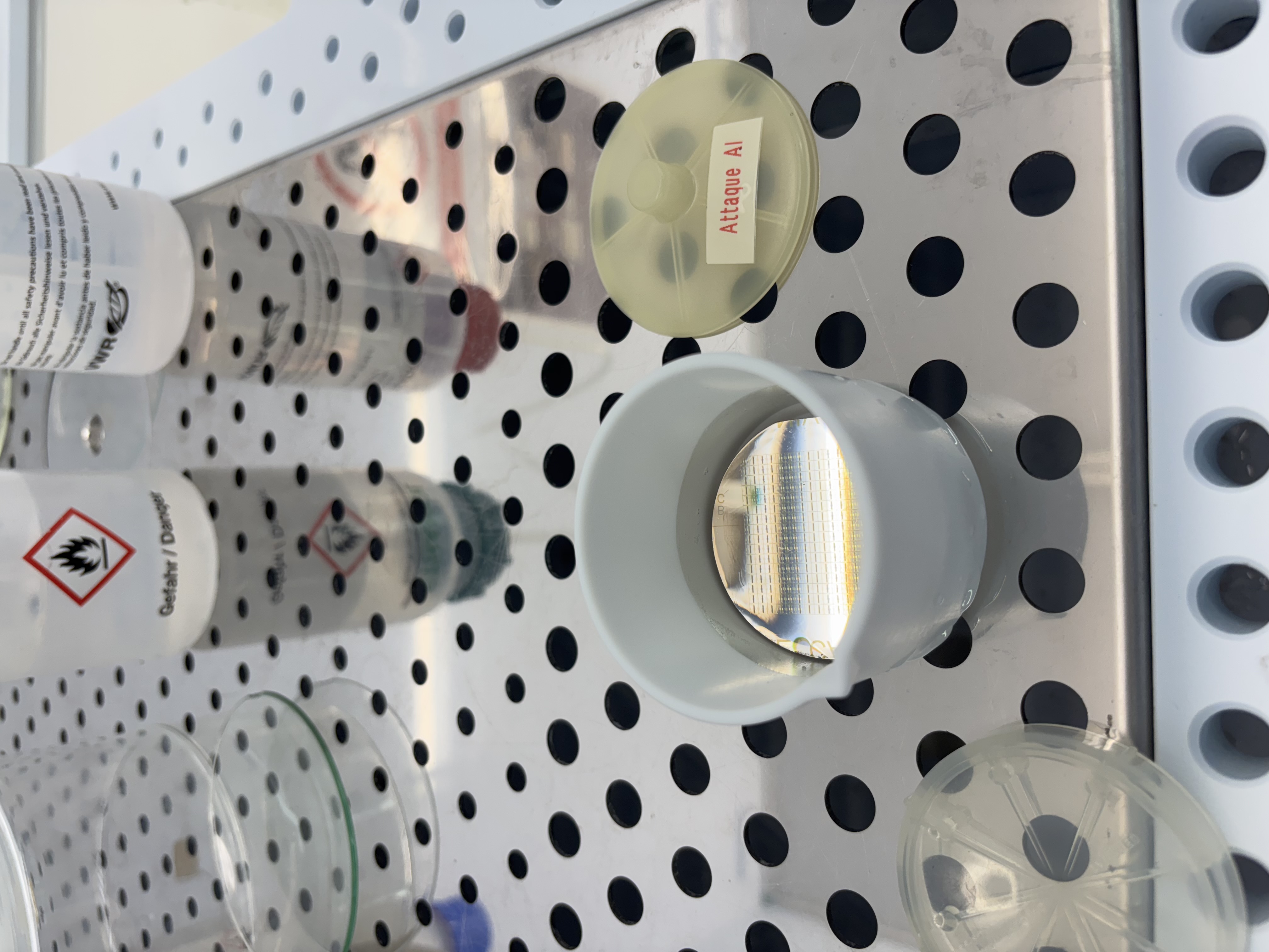
6. Gravure (seche et humide)
La gravure permet de retirer selectivement les materiaux non proteges par la resine photosensible.
Gravure humide (wet etching) :
- Isotrope (grave dans toutes les directions)
- Utilise des solutions chimiques specifiques : HF pour le SiO2, KOH pour le Si, acides pour les metaux
- Simple et economique mais moins precise pour les petites dimensions
Gravure seche (dry etching) :
- RIE (Reactive Ion Etching) : combine une attaque chimique (radicaux reactifs) et physique (bombardement ionique). Permet une gravure anisotrope (directionnelle) essentielle pour les motifs de petite dimension
- DRIE (Deep Reactive Ion Etching) : variante permettant de graver des structures profondes avec des flancs verticaux (procede Bosch)
Dans notre procede, la gravure du polysilicium et du metal a ete realisee pour definir les geometries des elements du capteur.
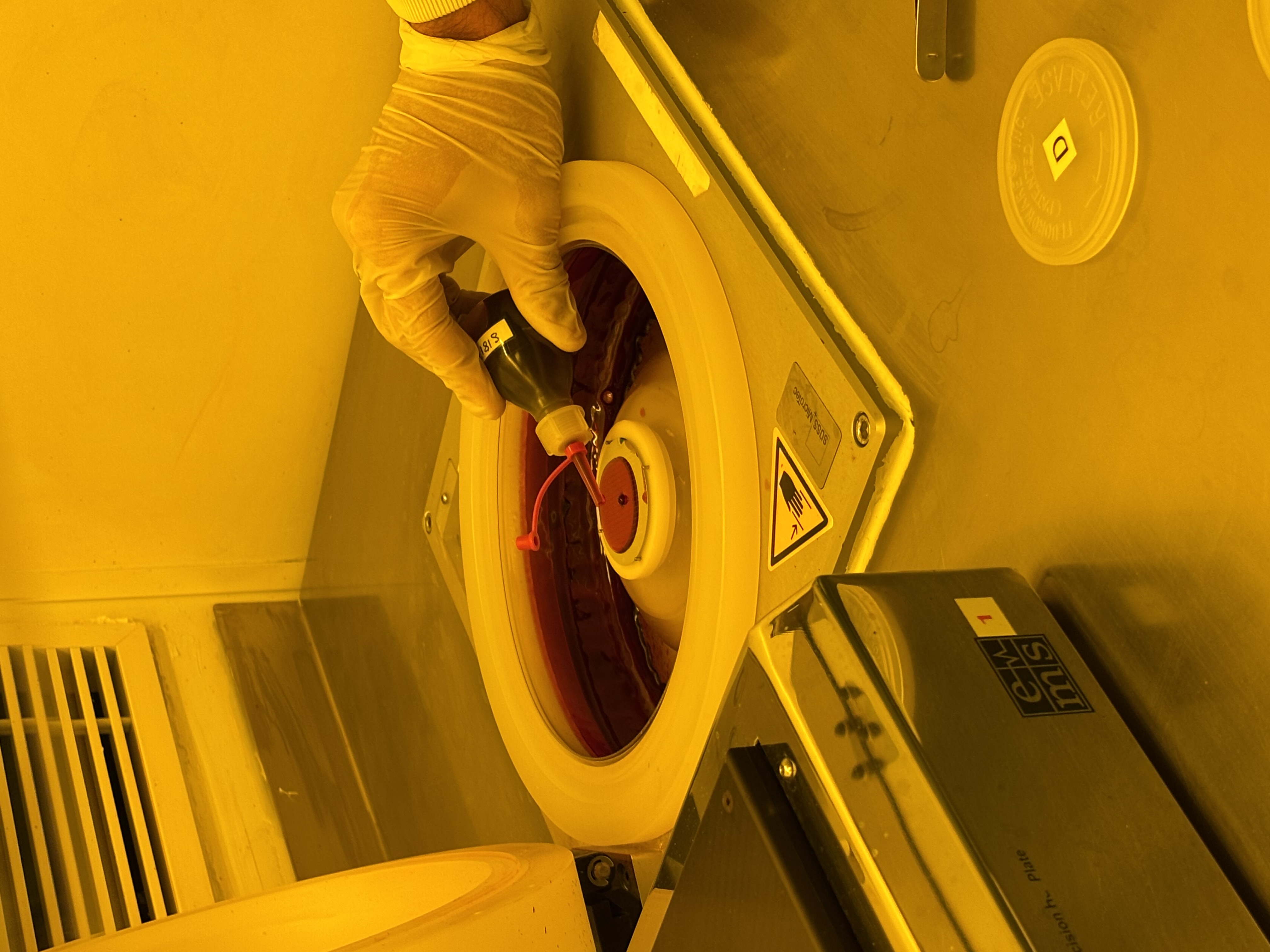
7. Decontamination organique et inspection
Entre les etapes critiques, des phases de nettoyage et d’inspection sont necessaires pour garantir la qualite du procede :
- Decontamination organique : elimination des residus de resine et des contaminants organiques par plasma O2 ou par voie chimique (acetone, isopropanol, melange piranha)
- Inspection optique : verification au microscope des motifs apres chaque etape de photolithographie pour s’assurer de la conformite dimensionnelle et de l’absence de defauts
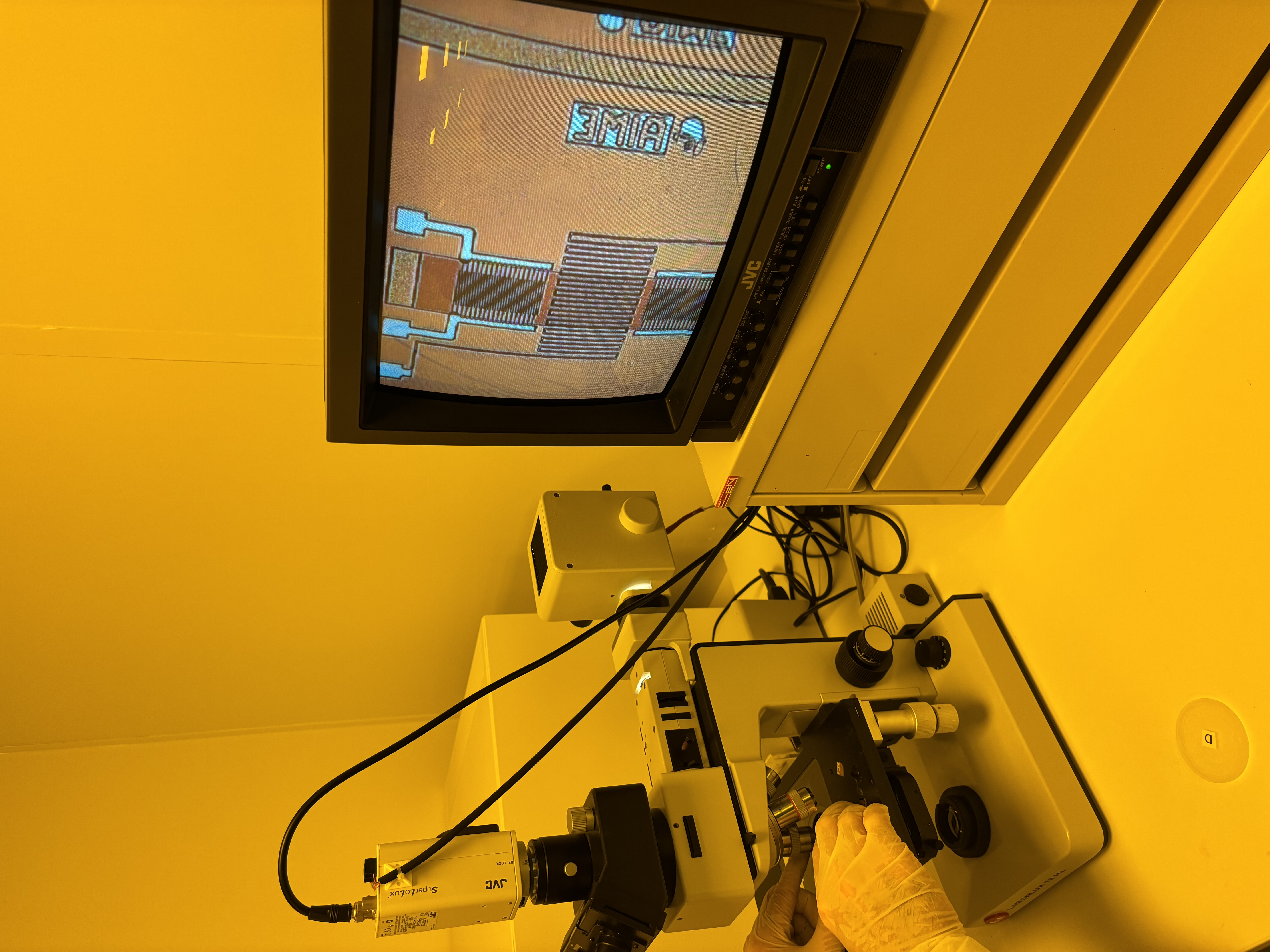
Inspection des motifs au microscope optique apres photolithographie
8. Metallisation
La metallisation consiste a deposer une couche d’aluminium (environ 300-500 nm) sur l’ensemble du wafer par PVD (evaporation ou pulverisation cathodique). Cette couche metallique formera les pistes de connexion electrique et les plots de contact du capteur.
L’aluminium est le metal de choix en microelectronique pour ses proprietes :
- Bonne conductivite electrique
- Excellente adherence sur SiO2
- Facilite de gravure
- Formation de contacts ohmiques avec le silicium dope
Apres depot, la photolithographie n3 et la gravure definissent les motifs metalliques finaux.
9. Recuit metallique (annealing)
Le recuit metallique est une etape thermique realisee apres la metallisation, typiquement a 400-450 degC sous atmosphere formante (N2/H2). Ses objectifs sont multiples :
- Ameliorer le contact metal/semiconducteur : former une interface de bonne qualite entre l’aluminium et le silicium dope pour obtenir des contacts ohmiques a faible resistance
- Reduire les contraintes mecaniques : relacher les contraintes internes dans les couches deposees
- Passiver les defauts d’interface : l’hydrogene de l’atmosphere formante passive les liaisons pendantes a l’interface Si/SiO2, ameliorant les proprietes electriques
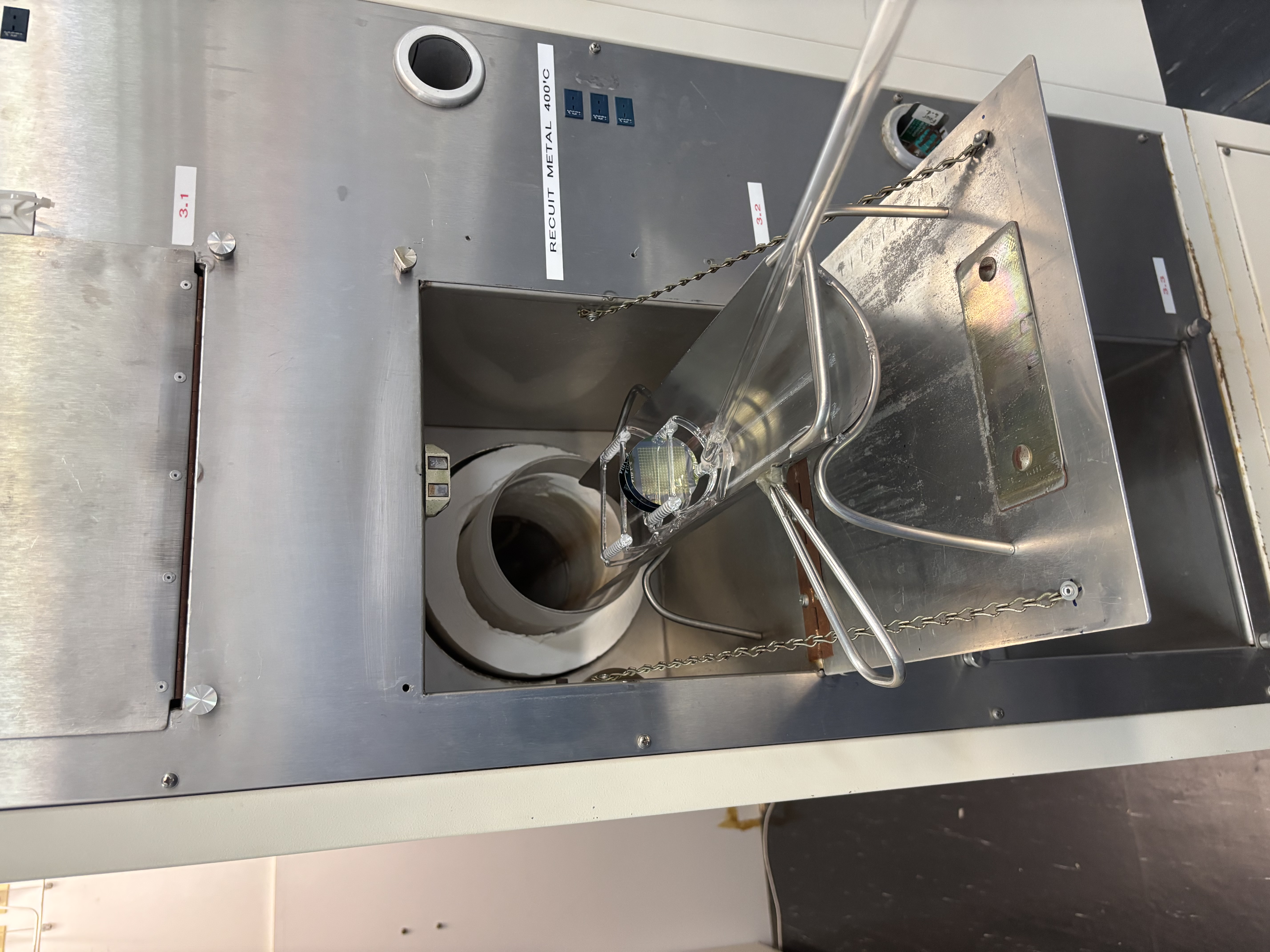
Four de recuit metallique - amelioration des contacts electriques
10. Fabrication MEMS/NEMS et conception du capteur
Le capteur de gaz que nous avons fabrique est un exemple de dispositif MEMS (Micro-Electro-Mechanical Systems). Il integre :
- Une resistance chauffante en polysilicium : permet de chauffer la zone sensible du capteur a la temperature optimale de fonctionnement (100-400 degC selon le gaz cible)
- Des electrodes interdigitees : paire d’electrodes metalliques en forme de peigne entre lesquelles sont deposees les nanoparticules sensibles
- Des plots de contact : permettent la connexion electrique du capteur au circuit de mesure
L’architecture du capteur exploite la variation de resistance des nanoparticules en presence du gaz cible. Lorsque les molecules de gaz s’adsorbent a la surface des nanoparticules, elles modifient la densite de porteurs de charge, ce qui se traduit par une variation mesurable de la resistance electrique entre les electrodes.
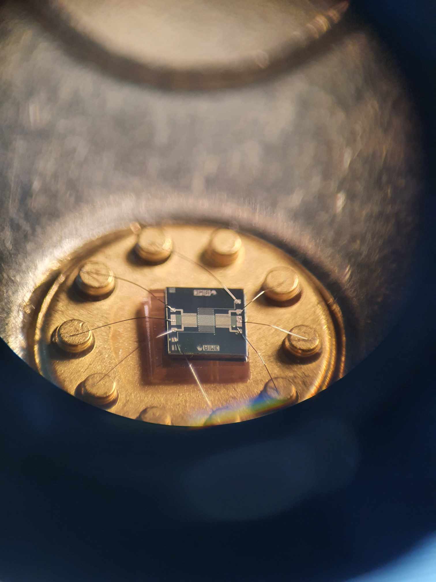
Vue au microscope du capteur de gaz fabrique - electrodes interdigitees et resistance chauffante
11. Assemblage et test du capteur
L’etape finale de fabrication consiste a assembler le capteur :
- Decoupe du wafer : separation des puces individuelles par clivage ou sciage
- Report sur boitier (packaging) : collage de la puce sur un support TO et connexion par wire-bonding (micro-soudure par fil d’or ou d’aluminium)
- Depot des nanoparticules : application de la solution collodale de nanoparticules par dielectrophorese (application d’un champ electrique alternatif pour aligner les nanoparticules entre les electrodes)
Les tests electriques sont realises sous pointes pour verifier :
- La continuite des pistes metalliques
- La valeur des resistances chauffantes
- L’isolation electrique entre les differents niveaux
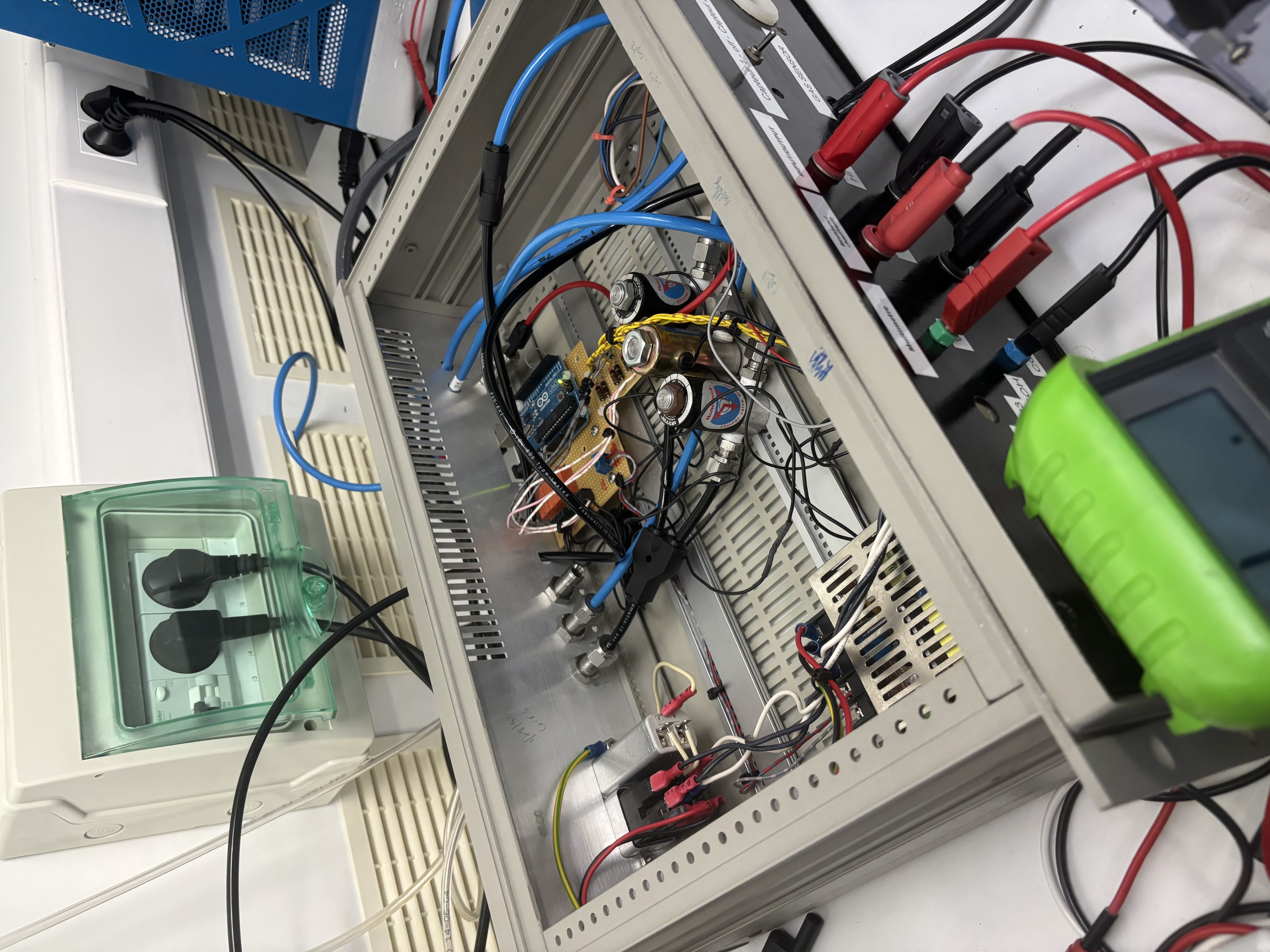
Des informations complementaires sur l’integration hardware sont disponibles dans la section Microcontroleur Hardware.
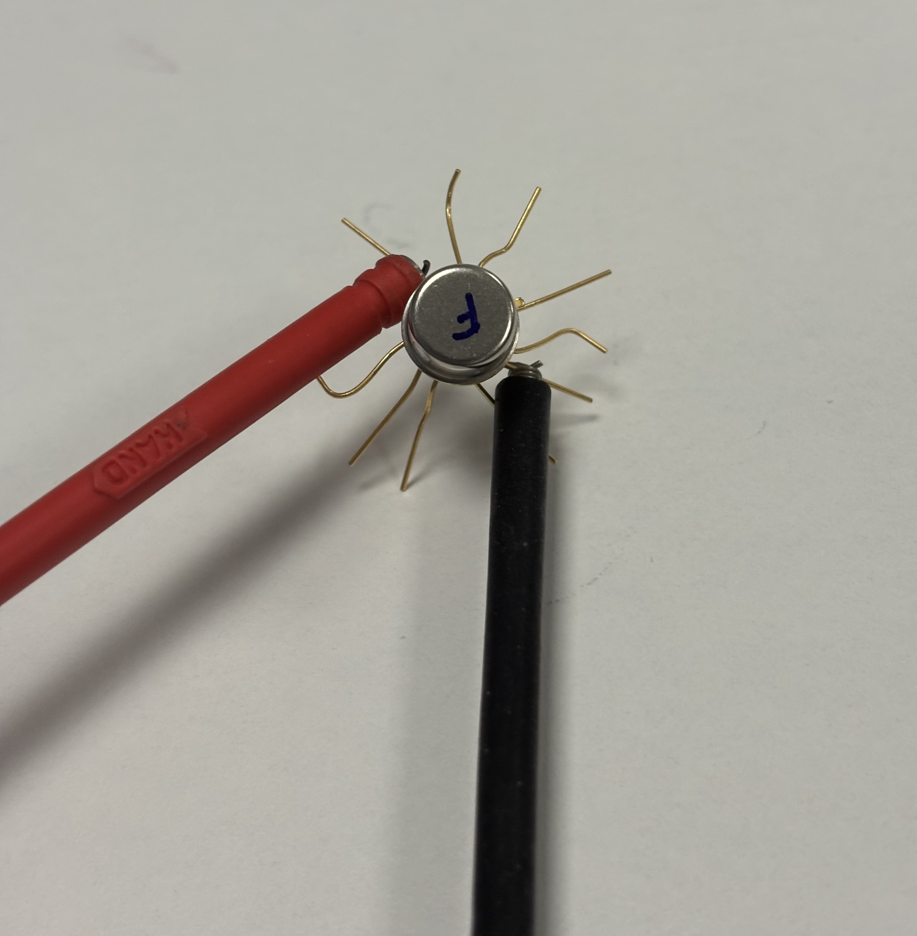
Test electrique du capteur assemble - verification des connexions et des resistances
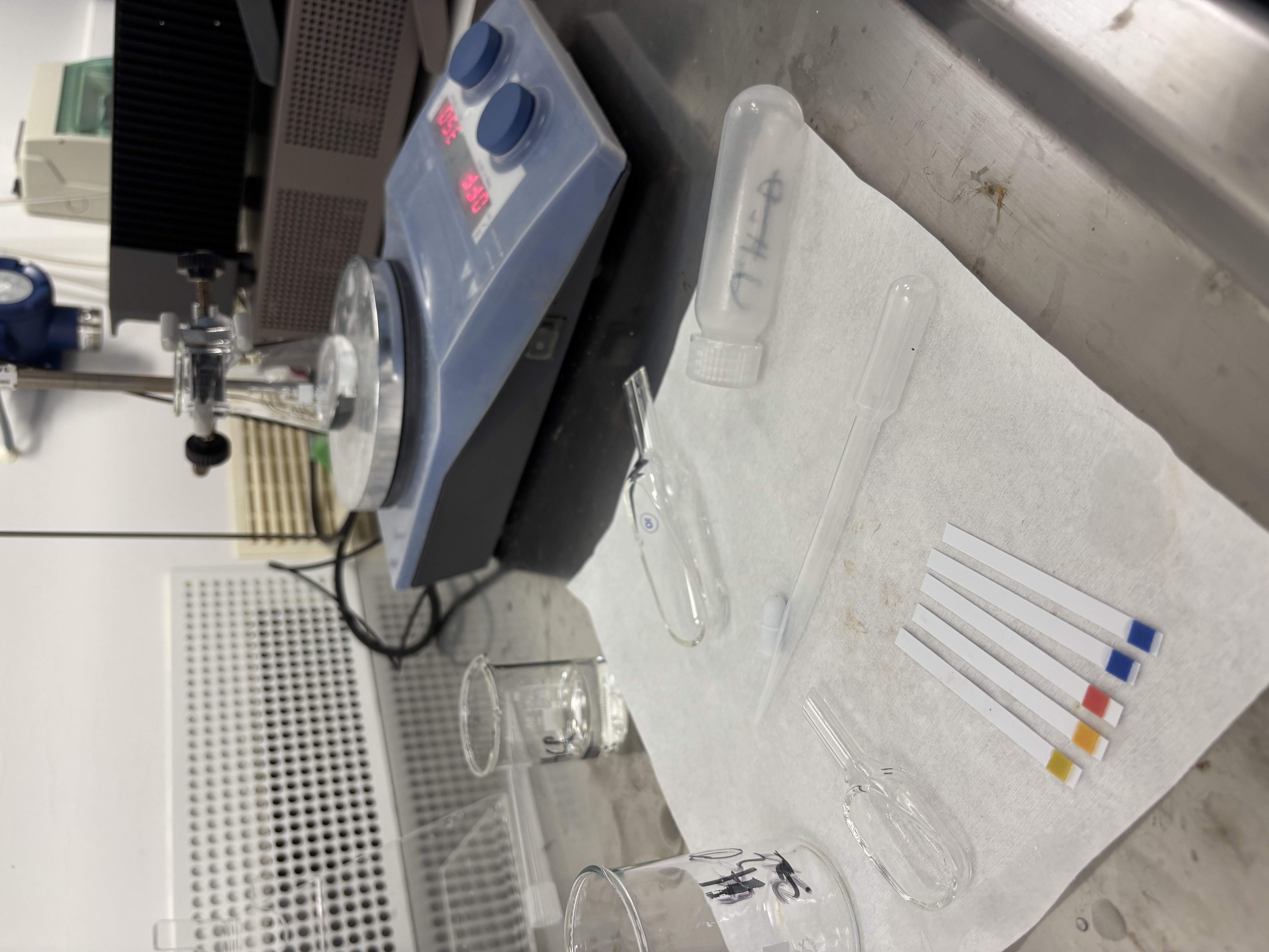
12. Mesures sous atmosphere controlee
La caracterisation finale du capteur a ete realisee dans une enceinte sous atmosphere controlee. Nous avons expose le capteur a deux gaz cibles :
- Ammoniac (NH3) : a une concentration de 0,1% dans l’air sec
- Ethanol (C2H6O) : a une concentration de 0,1% dans l’air sec
Le protocole de mesure consistait a :
- Etablir une ligne de base sous air sec pur
- Introduire le gaz cible a concentration connue
- Observer la variation de resistance du capteur
- Purger l’enceinte et observer le retour a la ligne de base
La tension de polarisation appliquee etait de 20V. L’acquisition des donnees a ete realisee via LabVIEW, permettant d’enregistrer en temps reel la variation de resistance du capteur. Les parametres evalues sont la sensibilite (amplitude de la variation de resistance), le temps de reponse, le temps de recouvrement et la selectivite entre les differents gaz.
Banc de mesure sous atmosphere controlee - caracterisation de la reponse du capteur aux gaz
Flux complet de fabrication
En resume, le flux de fabrication du capteur de gaz suit les etapes suivantes :
| Etape | Procede | Objectif |
|---|---|---|
| 1. Oxydation de masquage | Oxydation chimique (H2SO4 + H2O2) | Creer une couche protectrice sur le wafer |
| 2. Depot de polysilicium | LPCVD | Deposer la couche de polysilicium pour les resistances |
| 3. Dopage du polysilicium | Diffusion de phosphore (type N) | Rendre le polysilicium conducteur |
| 4. Photolithographie n1 | Gravure du polysilicium | Definir les motifs des resistances chauffantes |
| 5. Decontamination | Nettoyage organique | Eliminer les residus de resine |
| 6. Oxydation seche | Four d’oxydation | Creer la couche d’isolation |
| 7. Photolithographie n2 | Ouverture des contacts | Creer les acces electriques a travers l’oxyde |
| 8. Metallisation | PVD (aluminium) | Deposer les interconnexions metalliques |
| 9. Photolithographie n3 | Gravure du metal | Definir les pistes et plots de contact |
| 10. Recuit metallique | Four sous atmosphere formante | Ameliorer les contacts electriques |
| 11. Assemblage | Decoupe, wire-bonding, dielectrophorese | Mise en boitier et depot des nanoparticules |
| 12. Test | Mesure sous atmosphere controlee | Valider le fonctionnement du capteur |
PART D : ANALYSE ET REFLEXION
Connaissances et competences acquises
- Procedes de micro-fabrication : maitrise des etapes fondamentales (oxydation, depot CVD/PVD, dopage, photolithographie, gravure, recuit) et comprehension de leurs principes physico-chimiques
- Environnement de salle blanche : respect des protocoles stricts d’habillage et de manipulation, conscience des enjeux de contamination particulaire
- Conception de capteurs : comprehension de l’architecture d’un capteur de gaz resistif a base de nanoparticules et de son principe de fonctionnement
- Synthese chimique : participation a la synthese de nanoparticules et a leur depot par dielectrophorese
- Caracterisation electrique : mesure et analyse des performances du capteur sous atmosphere controlee
- Enregistrement et analyse de donnees : utilisation de LabVIEW pour l’acquisition en temps reel et traitement des resultats
Auto-evaluation
Ce cours a ete une veritable decouverte pour moi car je n’avais aucune competence prealable dans le domaine de la micro-fabrication. La comprehension des concepts chimiques et physiques a ete grandement facilitee par les enseignants, qui ont explique et guide chaque etape de maniere approfondie. J’ai ete suffisamment attentif pour assimiler et pratiquer l’ensemble des manipulations, ce qui m’a permis de ne rencontrer aucune difficulte majeure.
L’experience en salle blanche m’a permis de mesurer la complexite et la precision requises pour fabriquer des dispositifs microelectroniques. Chaque parametre (temperature, duree, pression, concentration) doit etre rigoureusement controle, ce qui demande une grande discipline et une attention constante.
J’ai egalement pris conscience de l’importance du travail en equipe dans un environnement de production : la coordination entre les membres du groupe est essentielle pour respecter le planning de fabrication et eviter les erreurs couteuses.
Mon avis
Avant ce cours, je ne savais pas exactement comment les capteurs etaient fabriques. Grace a ce module, j’ai vecu une premiere experience tres enrichissante qui m’a apporte de nouvelles competences. Meme si la micro-fabrication n’est pas exactement mon domaine de predilection, comprendre comment sont fabriques les capteurs que nous utilisons au quotidien est un atout precieux pour un ingenieur en electronique.
Nous avons commence les travaux pratiques avec un wafer de silicium deja partiellement prepare. Il aurait ete egalement interessant de partir d’un wafer vierge et de realiser la totalite du procede, y compris la gravure initiale des motifs sur silicium. Neanmoins, cette semaine intensive a ete extremement formatrice et m’a donne une vision concrete des enjeux de l’industrie microelectronique.
La combinaison de la fabrication en salle blanche, de la synthese chimique des nanoparticules et de la caracterisation electrique sous atmosphere controlee fait de ce module une experience pedagogique unique et tres complete. C’est un cours que je recommanderais a tout etudiant souhaitant comprendre les fondements de la microelectronique et de la fabrication de capteurs.
Lien vers le projet
Le projet complet du capteur de gaz, incluant la partie integration microcontroleur et l’interface de mesure, est disponible sur GitHub - Capteur de Gaz.