Introduction
Our project is to design a RISC type microprocessor, designated in VHDL on the Vivado development, simulation and implementation tool. This architecture promises faster program execution thanks to its 5 pipeline levels. This report will be structured to cover the different phases of the project. We will start by presenting the microprocessor architecture with the different key components such as the Arithmetic Logic Unit (ALU), the Register Bank, the Instruction Memory, the Data Memory, and other essential elements that will guide the design of our microprocessor. We will also address ALEA management, a crucial aspect of the design. Finally, we will analyze the synthesis results highlighting the optimizations made to increase the operating frequency as well as the reduction of its energy consumption.
RISC Microprocessor Architecture
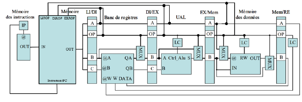
Microprocessor Component
In this part we will look at the architecture of a RISC microprocessor, however we will not go into details. Indeed there is a lot of documentation on this subject, which is clear and synthetic, they do not need a copy (which would be approximate). We will therefore present in a functional way the 5 elements present in our microprocessor the ALU, the data memory, the instruction memory and the register bank.
-
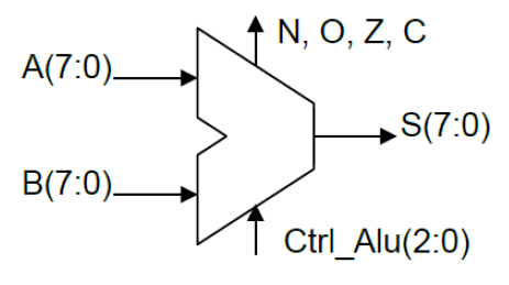
Arithmetic and Logic Unit
Functional Description
The Arithmetic Logic Unit (ALU) is the central component that allows the execution of arithmetic and logic operations of the microprocessor. The functional diagram of the ALU is given below in figure 1. The Control Bus (Ctrl_ALU) determines the type of operation to be performed. The ALU takes two inputs A and B of 8 bits, which will be the operands and S the result of the operation also on 8 bits. We also have 4 flags at the output, Negative, Carry, Zero and Overflow.
Functional Simulation
Below in Figure 2 is one of the functional simulations of our ALU. This simulation does not depend on time and implementation and only allows us to verify the logical operation of the circuit.
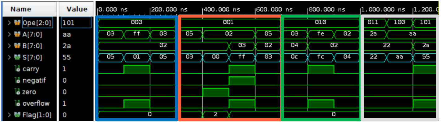
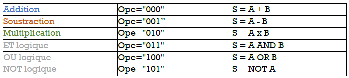
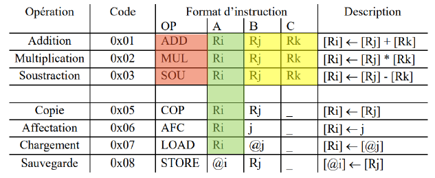
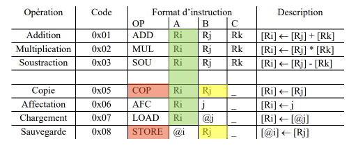
Below you will find table No. 1 allowing the link to be made between the control bus and the arithmetic and logical operations carried out.
The result of each operation is stored in the S output. Additionally, the component outputs information about the result in the form of flags in the Flag output, indicating whether an operation generated a carry, whether the result is negative, whether it is zero, or whether there was an overflow.
-
Register Bench
Functional Description
The Register Bank, integrated in our architecture, represents a fundamental element for temporary data storage during instruction execution. It consists of 16 8-bit registers, providing significant storage capacity for ongoing operations. This configuration allows simultaneous read access operations via ports QA and QB, as well as write operations via port W_in.
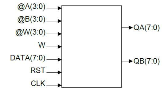
Functional Simulation
A simulation was performed to evaluate the reading, writing, and general behavior of the register bank. The values were manipulated to ensure proper data handling based on the clock. This includes scenarios such as simultaneous reading and writing to an output (bypass), or simply reading a register via the write port.
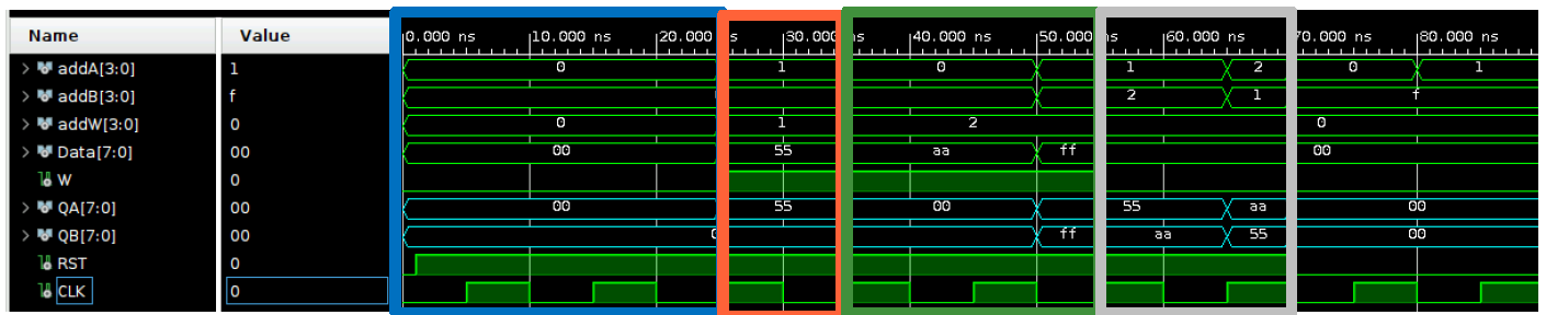
*Bypassing is a technique for reading and writing to a register at the same time. It is used in processors to improve efficiency by redirecting the calculated results directly to the next instructions that need them, without waiting for the register to be written.
-
Data Memory
Functional Description
Data memory is used to store temporary information needed for a program to operate. Operations on data memory include reading values stored at specific addresses and writing new values to those addresses.
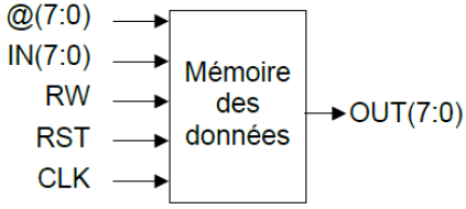
@(7:0) : Address at which read or write operations must be performed. IN(7:0) : Data input to be written to memory at the specified address. RW : Memory operation mode (0 for read, 1 for write). RST : Memory reset input. CLK : Clock input used to trigger memory operations. OUT(7:0) : Output returning the data read from the specified address.
Functional Simulation
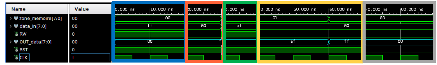
At each rising edge of the clock (CLK), the memory reacts according to the control (RW) and reset (RST) signals. In the event of a reset (RST at 1), the memory is reset to zero. In write mode (RW at 1), the input data (data) are written to the specified address. In read mode (RW at 0), the data located at the specified address are returned via the output (OUT).
-
Instruction Memory
Functional Description
Instruction memory stores the list of machine instructions that make up the program executed by the processor. Each instruction is associated with a specific memory address. Each instruction is represented on 32 bits and is accessible at a specific address in memory.
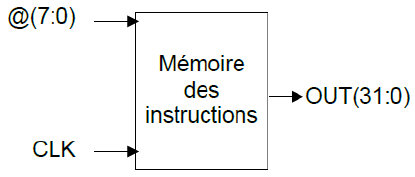
A [7 :0] : Input representing the address at which read operations must be performed. S [31 :0] : Output returning the 32-bit instruction read from the specified address
Functional Simulation
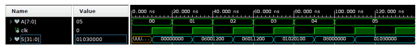
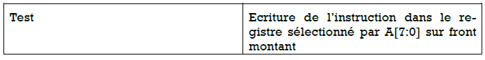
At each rising edge of the clock (clk), the memory reacts by returning the instruction located at the specified address via output S.
ALEA Management
Functional Description
We distinguish between data ALEA events and branch ALEA events. We will focus on data ALEA events. A data ALEA event is an event, this event is triggered by at least two instructions executing consecutively and in an incompatible manner. A first instruction modifies the value of a data item in a memory area, the second uses this memory area while the value has not been updated. To address this issue we have created a new component in our data path, which you can see below
If the component detects that the instruction sent by the instruction memory causes a ALEA with one of the instructions already present in the data path, then it blocks the instruction memory and sends NOPs in the data path. Once the ALEA is removed, it sends the blocked instruction and unlocks the instruction memory. It can be emphasized that the ALEA detection will only be done on the first 3 stages, in fact the register bank contains a bypass that allows reading and writing at the same time.
Detection Condition
We want to have the most general conditions possible to detect our ALEA events, this will avoid any kind of ambiguity and will allow us to simply manage all possible cases. We can start with the ALEA events caused by the MUL, SOU and ADD instructions.
If the incoming instruction is ADD, MUL or SOU then zone B and C must be different from zone A of the 3 instructions currently being executed. We do not trigger any ALEA on the instructions currently being executed that would be STORE. We can now continue with the ALEA caused by the COP and STORE instructions.
If the incoming instruction is COP or STORE, the B zone must be different from the A zones of the 3 instructions currently being executed. It can be emphasized that an incoming instruction of type AFC or LOAD cannot cause a ALEA event, and will only have an influence if they are already present in the data path. A ALEA event must also be detected only on instructions, so the opcode must be checked to avoid triggering a ALEA event on a NOP.
Functional Simulation
One point to emphasize is the NOP instruction, in fact a NOP must not do anything and by this we mean that it must not modify a register or a memory space, it can however enter the aluminum, cause a reading of the register bank or memory. From an external point of view, these interactions do not cause undesirable behavior on the part of the microprocessor, that being it causes unnecessary consumption.
- Simple ALEA
A first simple ALEA to perceive is a succession of two 2 AFCs followed by an addition of the two registers, this situation is simulated in the timeline below.
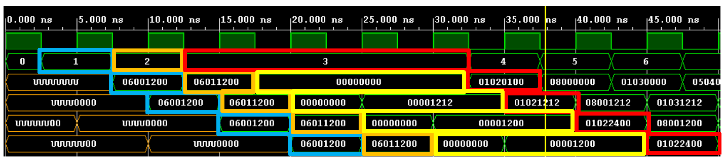
We send a first instruction “06001200” = R0<= 12
We send a second instruction “06001200” = R1<= 12
We send a third instruction “01020100” = R2<= R1+R0
Obviously the registers R0 and R1 are not up to date at the time of the addition so a “bubble” (here in yellow) is inserted, this bubble has a duration of 3 NOP.
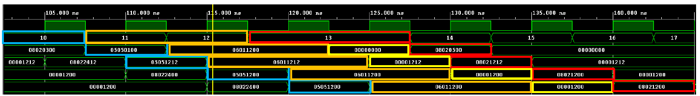
- Complex ALEA
A second example of ALEA is ALEA caused by two non-successive instructions, this situation is simulated in the timing diagram below.
We send a first instruction “01030000” = R3<= R0+R0
We send a second instruction “05040000” = R4<= R5
We send a third instruction “05040300” = R4<= R3
Here the ALEA number is between the third and the first instruction, the bubble (here in yellow) is equivalent to 2 NOPs. We see through this situation that the number of NOPs adapts according to the distance separating the ALEA numbers.
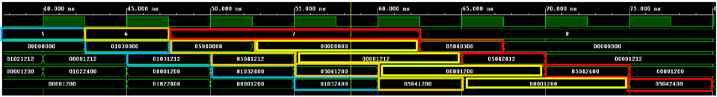
- Complementary ALEA
Finally, we can observe a last example of ALEA, it is a ALEA caused by two non-successive instructions, this situation is simulated in the timing diagram below.
We send a first instruction “05050100” = R5<= R1
We send a second instruction “06001200” = R0<= 12
We send a third instruction “06001200” = R0<= 12
We send a fourth instruction “08020500” = @02 <=R5
Here the ALEA number is between the fourth and first instructions the bubble (here in yellow) is equivalent to 1 NOP. We see through this situation that the number of NOPs adapts according to the distance separating the ALEA numbers and that we have treated all possible cases.
RISC Microprocessor Implementation
Implementation Choices
We could have implemented our components and made them work in different ways. For the components we simply designed them according to the indications of the subject. For the data path we decided to implement the 4 MUX delimiting the pipeline stages in the form of components. The discrete LC and simple MUX components were implemented concurrently directly in the data path. We believe that despite the loss of readability, this increases the performance of our microprocessor.
Analysis Upgrate Choices
Amelioration Axes
At the end of the project, several possibilities are available to us, we can improve our processor. For this, different opportunities present themselves to us, the first is to complete our instruction set in particular by adding functions such as logical OR, logical AND, etc. These functions are already integrated into our ALU, so we would have to modify our data path and our randomness management. Another area of improvement is the addition of jump and conditional jump type instructions. This area is interesting because it allows us to create more complex algorithms. A fourth area of improvement is to reduce the consumption of our microprocessor and its surface area as much as possible. Finally, a last possible area is the optimization of the system to increase its operating frequency. This is the choice we have decided to make, it is purely arbitrary.
Frequential Analysis and Critical Path
Our first Timing report indicates a MAX frequency of 65MHz, this result obviously does not satisfy us.
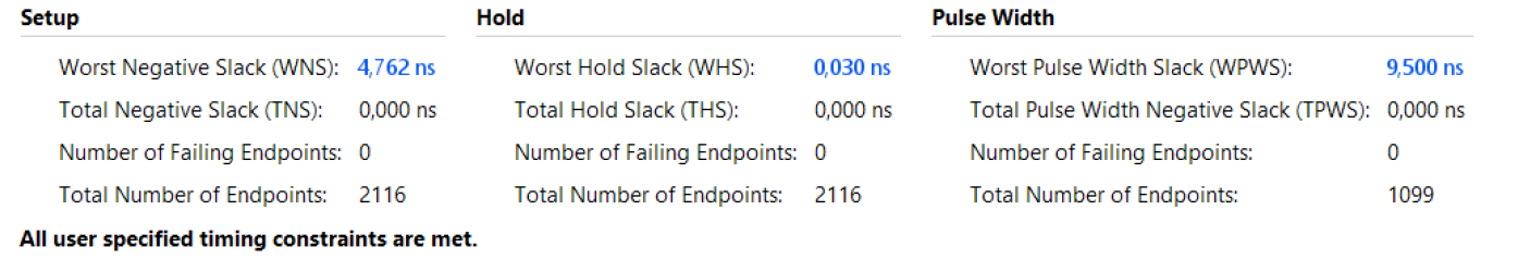
One might think that managing the falling edge randomness decreases our max frequency, however the critical path tells us that we should look at our memories. After optimizing our memory path, we have a clearer implementation schematic:
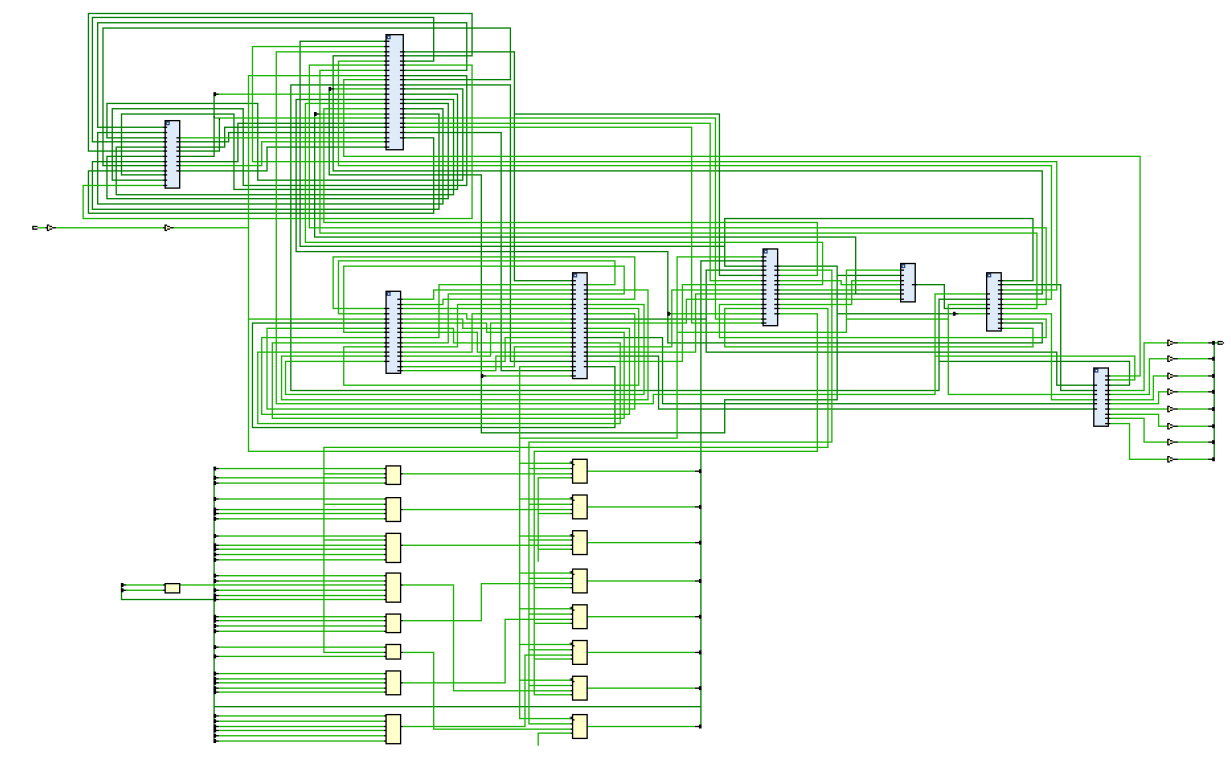
However our frequency is not higher, so we look again at our critical path:
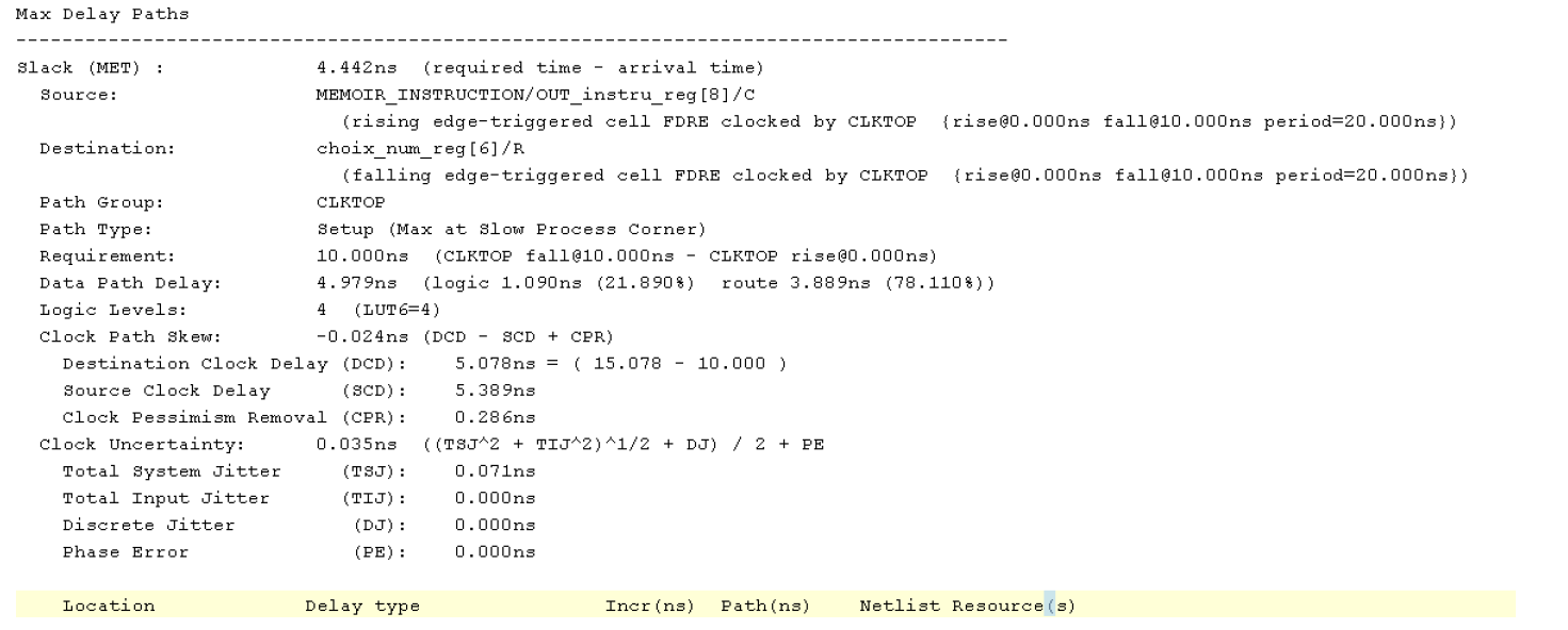
Despite our efforts we have not managed to reduce the propagation times through this path.
Performance
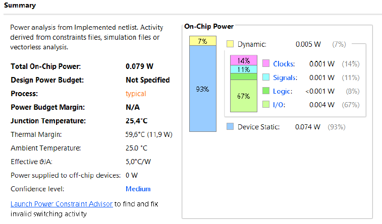
Energetic Consumption
Although our modifications did not increase the frequency, the energy consumption has decreased significantly. The decrease is of the order of 175%. Below you will find the summary power report.
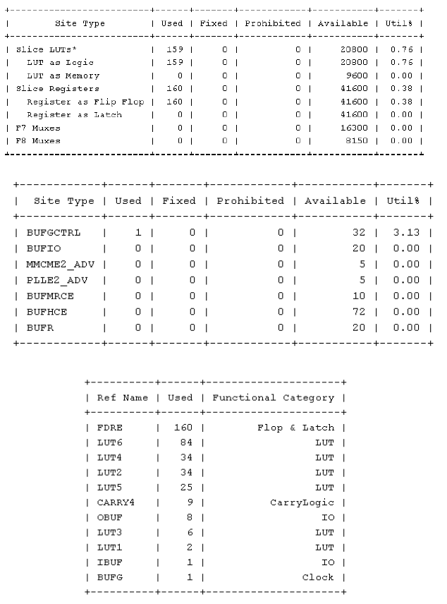
Component
Our consumption is intrinsically linked to our frequency and number of components. Below you will find extracts from the report indicating the different components used for our project and in what proportions.
Conclusion
The project was very interesting to carry out, the discovery of the Vivado software was instructive for us who had only worked on Qartus. This project also allowed us to apply in a concrete way the different notions seen during the modeling of digital components and architectures. We encountered many difficulties, particularly when trying to optimize critical paths, and we ultimately did not achieve our goals. Despite this failure, we are satisfied with our management of hazards. In addition, the approach allowed us to go further in the use of the different tools offered by Vivado, and on Vhdl design in general. Knowledge and understanding of the architecture of a microprocessor are also useful to us, we can describe this knowledge as transversal skills.