Introduction
This tutored project focused on designing and optimizing an antenna for IoT applications operating in ISM bands (433/868 MHz or 2.4 GHz). The project encompassed the complete design cycle from theoretical calculations and electromagnetic simulations to PCB fabrication and professional characterization using VNA and anechoic chamber measurements.
Project Overview
The goal was to develop a compact, efficient antenna for LoRa, Sigfox, WiFi, or Bluetooth applications. Key specifications included S11 < -10 dB, omnidirectional gain > 0 dBi, and 50Ω impedance matching.
Design Specifications
Target Frequencies:
- 433 MHz or 868 MHz (LoRa/Sigfox)
- 2.4 GHz (WiFi/Bluetooth)
- Bandwidth: ±10 MHz minimum
Performance Requirements:
- Return Loss: S11 < -10 dB
- Gain: > 0 dBi (omnidirectional)
- Impedance: 50Ω
- Efficiency: > 70%
Antenna Topologies Studied
For 433/868 MHz:
- Quarter-wave monopole (λ/4: 7-17 cm)
- Folded dipole
- Helical antenna (compact)
- PIFA (Planar Inverted-F Antenna)
For 2.4 GHz:
- Rectangular patch (3×4 cm)
- Printed dipole
- Meandered antenna (compact)
- Yagi (high gain)
Design and Simulation
Electromagnetic Modeling
We used CST Studio or HFSS for 3D electromagnetic simulation. The design process included:

Initial Dimensioning:
- Analytical formulas for patch/monopole dimensions
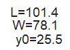
- Example: 2.4 GHz patch on FR-4 substrate (εr=4.4): L ≈ 3 cm, W ≈ 4 cm
Optimization:
- Parametric sweeps on critical dimensions
- S11 optimization at center frequency
- Radiation pattern analysis
- Impedance matching network design (stub, L-match)
Simulation Results:
- S11 < -15 dB at f₀
- Gain: 6-8 dBi (patch), 2 dBi (monopole)
- 3D radiation pattern
- Input impedance: Z = 50 + j0 Ω

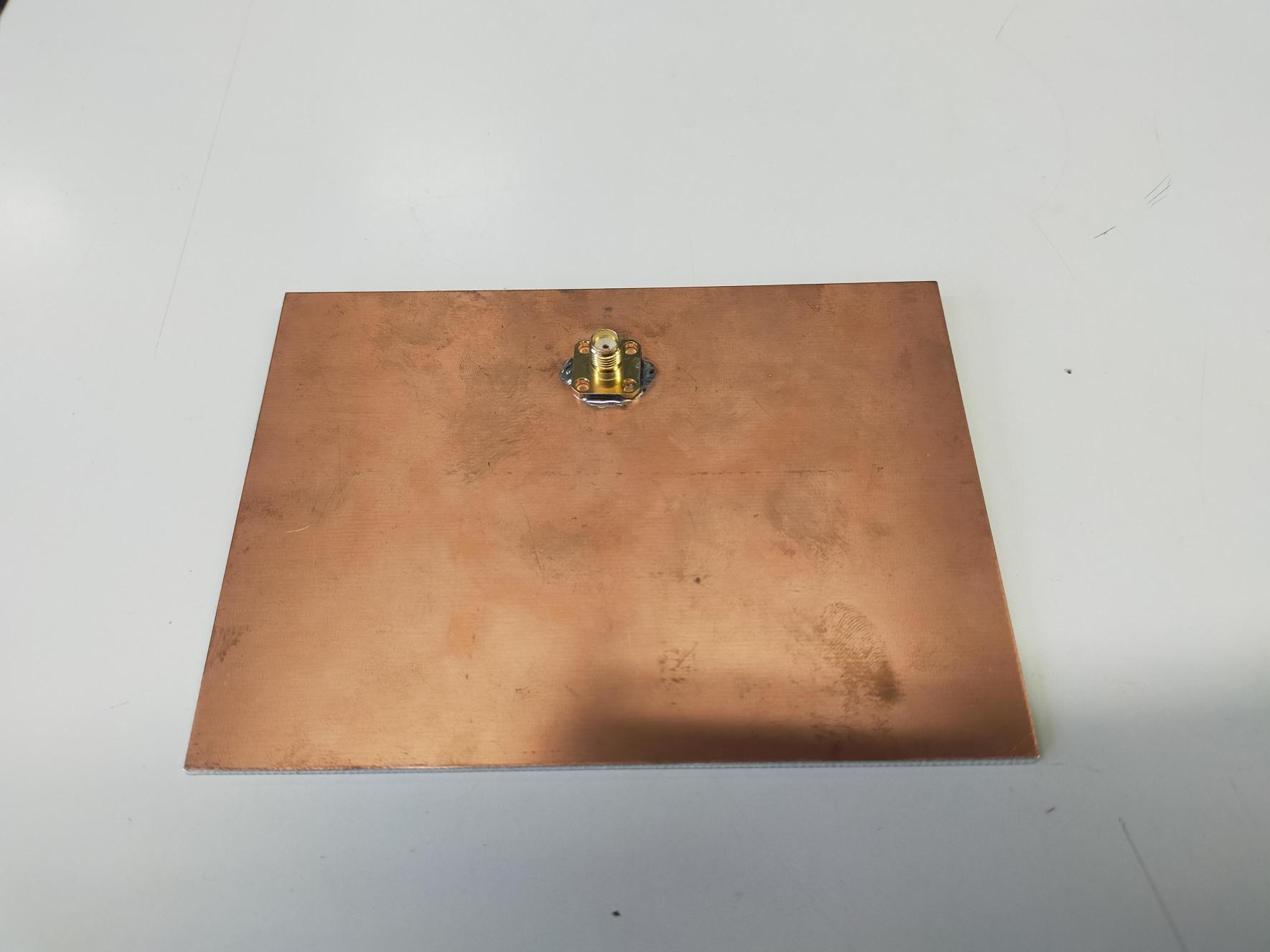
PCB Fabrication
Design and Manufacturing
- Designed in KiCad/Altium Designer
- Precise layout matching optimized dimensions
- Substrate: FR-4 (εr=4.4) or Rogers for better performance
- Manufactured by PCBWay/JLCPCB
- SMA connector soldering
- Visual inspection and continuity testing
Characterization and Testing
VNA Measurements
Using Vector Network Analyzer with SOLT calibration:
- S11 parameter (reflection coefficient) vs frequency
- Smith chart for impedance analysis
- Comparison simulation vs measurement
- Bandwidth verification
Anechoic Chamber Testing
Professional RF chamber measurements:
- Radiation patterns (E-plane, H-plane)
- Absolute gain measurement
- Polarization characteristics
- Cross-polarization levels


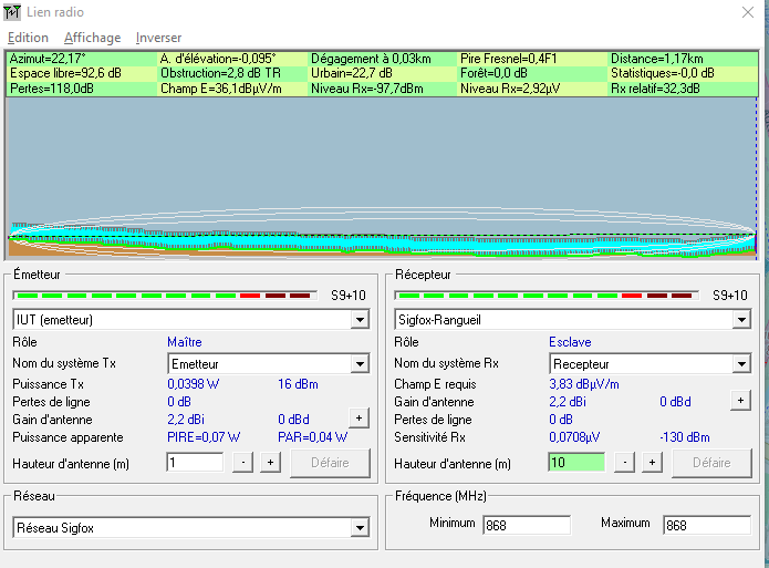
Real-World Link Testing
- Connected to LoRa/WiFi module
- Range testing with RSSI measurements
- Comparison with commercial antenna
- Performance validation in operating environment
Results and Analysis
The fabricated antenna met specifications with S11 < -12 dB at the target frequency. Measured gain matched simulations within ±1 dB. Real-world link tests demonstrated effective communication range for the target IoT application.
Key learnings included the impact of substrate properties on performance, importance of precise manufacturing tolerances, and ground plane effects on radiation patterns.
Conclusion
This project provided comprehensive hands-on experience in RF antenna design, from theoretical analysis through professional characterization. We successfully designed, fabricated, and validated a functional antenna for IoT applications, demonstrating the complete engineering workflow for wireless communication systems.
PART B: EXPÉRIENCE, CONTEXTE ET FONCTION (Cahier des charges)
Spécifications techniques
Fréquence :
- 433 MHz (LoRa EU)
- 868 MHz (Sigfox, LoRa EU)
- 2.4 GHz (WiFi, Bluetooth, Zigbee)
- Bande passante : ≥10 MHz
Performances :
- Adaptation : S11 < -10 dB
- Gain : >0 dBi (omnidirectionnel) ou >5 dBi (directif)
- Polarisation : linéaire verticale (ou circulaire si GNSS)
- Impédance : 50Ω
Contraintes :
- Compact (IoT portable)
- Faible coût (PCB FR-4 acceptable)
- Fabrication simple
Types d’antennes possibles
433/868 MHz :
- Monopole λ/4 (7-17 cm)
- Dipole replié
- Hélice (compacte)
- PIFA (Planar Inverted-F Antenna)
2.4 GHz :
- Patch rectangulaire (3×4 cm)
- Dipole imprimé
- Antenne méandre (compacte)
- Yagi (gain élevé)
PART C: ASPECTS TECHNIQUES (Méthodologie)
Phase 1 : Étude et conception (15h)
Recherche bibliographique :
- État de l’art antennes IoT
- Choix topologie (patch, monopole, etc.)
Dimensionnement théorique :
- Formules analytiques (longueur λ)
- Calcul dimensions initiales
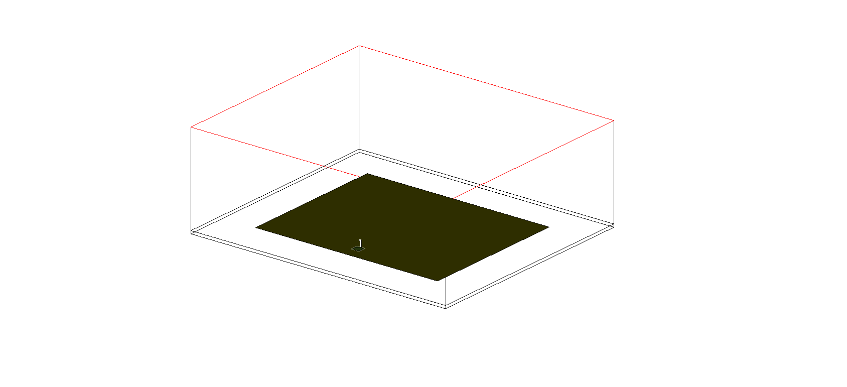
- Exemple patch 2.4 GHz : L ≈ 3 cm, W ≈ 4 cm sur FR-4
Adaptation :
- Design matching network (stub, L-match)
- Calcul Smith chart
Phase 2 : Simulation EM (15h)
Modélisation 3D :
- Logiciel : CST, HFSS, ou MMANA (Yagi)
- Géométrie complète (substrat, plan de masse)
- Maillage adapté
Optimisation :
- Paramétrage dimensions
- Sweep fréquentiel
- Optimisation S11, gain, diagramme
Résultats simulation :
- S11 < -15 dB à f₀
- Gain 6-8 dBi (patch), 2 dBi (monopole)
- Diagramme rayonnement 3D
- Impédance Z = 50 + j0 Ω
Phase 3 : Réalisation (10h)
PCB :
- Schéma KiCad/Altium
- Layout précis (dimensions optimisées)
- Fabrication (PCBWay, JLCPCB)
- Substrat : FR-4 (εr=4.4) ou Rogers (meilleur)
Assemblage :
- Soudure connecteur SMA
- Vérification continuités
- Inspection visuelle
Phase 4 : Caractérisation (10h)
Mesures VNA :
- Calibration SOLT
- S11 : adaptation vs fréquence
- Smith chart : impédance
- Comparaison simulation vs mesure
Chambre anéchoïque :
- Diagramme rayonnement (plan E, H)
- Gain absolu
- Polarisation
Tests liaison :
- Module LoRa/WiFi connecté
- Mesure portée (RSSI)
- Comparaison antenne commercial
PART D: ANALYSE ET RÉFLEXION
Livrables
- Rapport technique (30 pages) : étude, simulations, réalisation, mesures
- Fichiers simulation (CST/HFSS)
- Fichiers PCB (Gerber)
- Présentation orale (20 min)
- Démonstration liaison radio
Évaluation
- Qualité conception et simulation (25%)
- Réalisation PCB (20%)
- Mesures et validation (25%)
- Rapport et documentation (20%)
- Présentation orale (10%)
Compétences acquises
- Conception antennes RF professionnelle
- Simulation EM 3D
- Mesures VNA et chambre anéchoïque
- Gestion projet en autonomie
- Documentation technique
Débouchés
- Ingénieur antennes (IoT, télécom)
- Concepteur RF
- R&D objets connectés
📚 Cahier des charges
Spécifications techniques
Fréquence de travail :
- Options : 433 MHz, 868 MHz, 2.4 GHz
- Selon application IoT choisie
- Bande passante : ±10 MHz minimum
Performances :
- Adaptation : S11 < -10 dB
- Gain : > 0 dBi (omnidirectionnelle)
- Polarisation : linéaire (typiquement)
- Efficacité : > 70%
Contraintes :
- Compacte pour objets connectés
- Fabrication PCB standard
- Coût réduit
- Robustesse mécanique
Applications visées
IoT basse consommation :
- LoRa (868 MHz Europe, 915 MHz US)
- Sigfox (868 MHz Europe)
- WiFi 2.4 GHz
- Zigbee 2.4 GHz
- Bluetooth 2.4 GHz
Cas d’usage :
- Capteurs environnementaux
- Smart agriculture
- Smart city
- Wearables
- Asset tracking
🛠️ Réalisation du projet
Phase 1 : Étude et choix de conception
Analyse des besoins
- Définir l’application cible
- Contraintes mécaniques
- Environnement d’utilisation
- Budget
Choix du type d’antenne
Options étudiées :
- Antenne patch (microstrip) :
- Compacte, planaire
- Fabrication PCB facile
- Bande passante limitée
- Gain moyen (5-7 dBi)
- Antenne monopole λ/4 :
- Omnidirectionnelle
- Simple
- Nécessite plan de masse
- Gain ~2 dBi
- Antenne IFA (Inverted-F) :
- Très compacte
- Bonne pour GSM/WiFi
- Accordable
- Largeur de bande ajustable
- Antenne dipôle plié :
- Bande passante améliorée
- Fabrication PCB
- Omnidirectionnelle
- Antenne PIFA (Planar IFA) :
- Très compacte
- Multi-bande possible
- Intégration facile
- Smartphones, IoT
Choix justifié : Sélection basée sur compromis :
- Performances RF
- Encombrement
- Facilité de fabrication
- Coût
Phase 2 : Dimensionnement théorique
Calculs de base
Longueur d’onde : \(\lambda = \frac{c}{f} = \frac{3 \times 10^8}{f}\)
Exemples :
- 433 MHz : λ ≈ 69 cm
- 868 MHz : λ ≈ 34.5 cm
- 2.4 GHz : λ ≈ 12.5 cm
Dimensions antenne : Selon type choisi (λ/4, λ/2, patch, etc.)
Substrat PCB :
- FR-4 (εr ≈ 4.3) : économique
- Rogers (εr stable) : performances
- Épaisseur : 0.8, 1.6 mm typique
Longueur d’onde guidée : \(\lambda_g = \frac{\lambda_0}{\sqrt{\varepsilon_{reff}}}\)
Adaptation d’impédance
Objectif : 50Ω
- Ligne microstrip 50Ω
- Stub d’adaptation si nécessaire
- Connecteur SMA ou U.FL
Phase 3 : Simulation EM
Logiciels utilisés
MMANA-GAL :
- Antennes filaires (dipôle, Yagi)
- Méthode des moments
- Gratuit
- Rapide
CST Microwave Studio :
- Simulation 3D complète
- Temps domaine ou fréquentiel
- Précis
- Professionnel
HFSS :
- Méthode éléments finis (FEM)
- Haute précision
- Standard industrie
AWR (Applied Wave Research) :
- Suite complète RF
- Antenne + circuit
- Momentum (EM planar)
Paramètres simulés
Adaptation (S11) :
- Fréquence de résonance
- Bande passante -10 dB
- TOS (VSWR)
Diagramme de rayonnement :
- 2D (plans E et H)
- 3D
- Gain maximum
- Ouverture à -3 dB
Impédance d’entrée :
- Partie réelle et imaginaire
- Smith chart
- Évolution fréquentielle
Efficacité :
- Pertes diélectriques
- Pertes ohmiques
- Efficacité de rayonnement
Optimisation
Variables ajustables :
- Dimensions géométriques
- Position stub d’adaptation
- Largeur de lignes
- Plan de masse
Objectif :
- S11 < -10 dB sur bande
- Gain maximum
- Diagramme adapté à l’application
Phase 4 : Réalisation PCB
Design du PCB
Logiciel CAO :
- Altium Designer
- KiCad
- Eagle
Couches :
- Top : antenne + lignes RF
- Bottom : plan de masse
- 2 couches typiquement
Éléments :
- Antenne dimensionnée
- Ligne 50Ω vers connecteur
- Connecteur SMA ou U.FL
- Points de test
- Découplage si électronique intégrée
Fabrication :
- Génération Gerber
- Fabricant (JLCPCB, PCBWay, etc.)
- Délai : 1-2 semaines
- Coût : quelques euros
Assemblage
Composants :
- Connecteur SMA
- Composants d’accord (si nécessaire)
Soudure :
- Fer à souder température contrôlée
- Flux
- Inspection visuelle
Mécanique :
- Support si nécessaire
- Boîtier de protection
- Câble d’alimentation
Phase 5 : Caractérisation
Mesures au VNA (Analyseur de Réseau Vectoriel)
Calibration :
- SOLT (Short, Open, Load, Thru)
- Au plan du connecteur de l’antenne
Paramètres S11 :
- Fréquence de résonance réelle
- Bande passante mesurée
- TOS (VSWR)
- Comparaison simulation/mesure
Smith chart :
- Impédance d’entrée
- Évolution fréquentielle
- Validation adaptation
Mesures en chambre anéchoïque
Diagramme de rayonnement :
- Setup antenne sous test + antenne référence
- Rotation 360° (plan H et E)
- Mesure puissance reçue
- Tracé du diagramme
Gain absolu :
- Méthode de substitution
- Comparaison avec antenne étalon
- Calcul du gain
Polarisation :
- Mesure composantes H et V
- Rapport axial (si circulaire)
Tests en conditions réelles
Bilan de liaison radio :
- Émetteur à puissance connue
- Distance variable
- Mesure RSSI
- Comparaison avec théorie
Portée effective :
- Module LoRa/WiFi/BT
- Environnement indoor/outdoor
- Obstacles
- Validation cahier des charges
Phase 6 : Analyse et optimisation
Comparaison simulation/mesure
Écarts typiques :
- Décalage fréquentiel (εr imprécis)
- Différences de gain (pertes réelles)
- Diagramme (influence environnement)
Corrections possibles :
- Ajustement dimensionnel
- Stub d’adaptation
- Optimisation mécanique
Améliorations
Si performances insuffisantes :
- Tuning par stub variable
- Modification dimensions
- Changement de substrat
- Nouvelle itération
Si performances OK :
- Miniaturisation
- Multi-bande
- Polarisation circulaire
📊 Livrables du projet
Documentation technique
- Cahier des charges :
- Spécifications
- Contraintes
- Application visée
- Étude théorique :
- Calculs dimensionnels
- Choix justifiés
- État de l’art
- Simulations :
- Screenshots CST/HFSS
- Paramètres S11
- Diagrammes de rayonnement
- Courbes de gain
- Design PCB :
- Schémas
- Layout
- Fichiers Gerber
- Nomenclature
- Mesures :
- Protocoles
- Résultats VNA
- Diagrammes mesurés
- Tests de portée
- Analyse :
- Comparaison simulation/mesure
- Validation cahier des charges
- Améliorations proposées
- Rapport final :
- 30-50 pages
- Structuré et illustré
- Bibliographie
Réalisations pratiques
- PCB d’antenne fonctionnel
- Prototype assemblé
- Démonstration de liaison
- Poster de présentation
Soutenance
- Présentation 15-20 minutes
- Support PowerPoint
- Démonstration live
- Questions jury
💻 Outils utilisés
Simulation
- MMANA-GAL : Filaires
- CST Microwave Studio : 3D EM
- HFSS : FEM précision
- AWR : Suite RF complète
Planification
- Radio Mobile : Couverture
- Google Earth : Terrain 3D
- SPLAT! : Open source
Conception PCB
- Altium Designer
- KiCad
- Eagle
Mesure
- Analyseur de réseau vectoriel (VNA)
- Chambre anéchoïque
- Générateur RF
- Analyseur de spectre
🔗 Liens avec les cours
- Antennes et Propagation (S4) : Base théorique
- Propagation Hyperfréquences (S3) : Adaptation
- Circuits Hyperfréquences (S3) : Conception RF
- ER : Réalisation PCB
💡 Exemples de réalisations
Antenne patch 2.4 GHz
- Substrat FR-4, 1.6 mm
- Dimensions : 38×30 mm
- Gain : 6 dBi
- S11 < -15 dB @ 2.44 GHz
- Application : WiFi, Zigbee
Antenne monopole 868 MHz
- λ/4 sur PCB
- Longueur : 8.2 cm
- Plan de masse 10×10 cm
- Omnidirectionnelle
- Application : LoRa, Sigfox
Antenne IFA 2.4 GHz
- Compacte : 25×8 mm
- Intégrée dans boîtier
- Bande passante 2.4-2.5 GHz
- Application : Bluetooth, WiFi
📖 Compétences développées
- Conception d’antennes RF
- Simulation électromagnétique 3D
- Design de PCB RF
- Mesure avec VNA
- Analyse de performances
- Optimisation itérative
- Gestion de projet technique
- Rédaction de documentation
⚠️ Points d’attention
Simulation
- Modèle de substrat précis
- Maillage suffisant
- Conditions aux limites
- Temps de calcul
Fabrication
- Précision dimensionnelle
- Qualité du substrat
- Soudure propre du connecteur
- Protection mécanique
Mesures
- Calibration VNA cruciale
- Environnement sans réflexions
- Câbles de qualité
- Connectique serrée
Validation
- Tests multiples
- Environnements variés
- Comparaison avec théorie
- Reproductibilité
🎯 Critères d’évaluation
- Respect du cahier des charges (25%)
- Qualité des simulations (20%)
- Réalisation pratique (20%)
- Mesures et validation (20%)
- Rapport et présentation (15%)
📚 Ressources
- Balanis “Antenna Theory”
- Application notes fabricants
- IEEE Antennas and Propagation Magazine
- Tutoriels CST/HFSS
- Forums RF (edaboard, etc.)
Project Documentation
Below are the three phases of the antenna project documentation. You can scroll through each PDF side by side.